pixalynx/pixal-nfc-card
This code defines React components representing specific electronic hardware components—namely, a 100-ohm SMD resistor, a surface-mount LED, and a chip with labeled pins—each modeled with detailed footprints, 3D CAD models, and manufacturer part information for PCB design.
- Version
- 1.1.0
- License
- unset
- Stars
- 0
fabrication/rev-b/FABRICATION.md
PCB

Schematic

# Revision B fabrication and assembly specification

Status: CAM REVIEW / PROTOTYPE CANDIDATE. Production release requires the RF results in RF-VALIDATION.md. Use only the checked archive produced by `bun run fab`. Raw `tsci export` adds unwanted antenna paste and a false L1 placement.

## Bare board

- Finished outline 85.60 × 54.00 mm, radius 3.18 mm, routed; origin at board centre; coordinates in mm, top view.
- Two-layer FR-4, finished PCB thickness 0.60 mm (supplier capability ±0.10 mm); 1 oz copper each layer; ENIG; black solder mask, white top silk.
- Bottom winding: 5 turns, 0.45 mm copper / 0.45 mm gap. No copper thieving, planes, metallic graphics, part markings or conductive backing inside RF keepout on either face. Two intentional top antenna feeds cross the winding region.
- Both antenna terminal holes: finished plated hole Ø0.30 mm, copper Ø0.80 mm; 0.25 mm radial annular ring. These are interlayer antenna connections, not component insertion holes. No solder paste or solder fill at either terminal, either face. Mask openings are intentional; do not add exposed copper to the winding.
- U1 manufacturer's land pattern retained: four 0.20 × 0.60 mm lands and central 0.20 × 1.60 mm land. NC pads 1, 2, 5 receive paste for mechanical attachment but remain electrically isolated. Do not enlarge pads to a generic 0.25 mm minimum without rerouting/review.
- **CAM gate:** obtain written acceptance of these 0.20 mm-wide lands and mask geometry; they are below JLCPCB's generic published 0.25 × 0.25 mm SMD-pad guidance. The manufacturer's footprint controls package fit.

## Assembly and stencil

Use JLCPCB **Standard PCBA**, top side only. Economic's published thickness range starts at 0.8 mm. Standard requires rails and fiducials and a ≥70 × 70 mm carrier; use factory panelization per PANELIZATION.svg below. The manufacturing archive contains SINGLE-UNIT Gerbers and SINGLE-UNIT CPL, not panel Gerbers. Factory must replicate geometry and placement consistently.

Only placed part: U1, STMicroelectronics ST25TN01K-AFH5, UFDFPN5 1.7 × 1.4 mm, C3303589, quantity 1 per card. L1 is etched copper; R1/D1 have been removed entirely. No substitute is authorized by this release.

Top stencil: specify 0.10 mm laser-cut foil with the supplied 1:1 apertures; four 0.20 × 0.60 mm and one 0.20 × 1.60 mm. Area ratios are 0.75 and 0.889 respectively; width/foil ratio 2.0. Do not apply the previous 70%-per-axis aperture scaling (49% of pad area). Factory stencil engineering must confirm paste/process suitability; use SPI and inspect hidden joints as applicable. Bottom stencil is empty and must not be ordered. NC central land is NOT a ground pad.

CPL: U1 centre (+13.50, 0.00), top, rotation 180°. This angle is the tscircuit footprint rotation, not a guarantee of supplier library orientation. Compare factory assembly preview to these **physical pin positions**: pin 1 NC3 (+13.90,+0.50), pin 2 NC1 (+13.50,0), pin 3 AC0 (+13.10,+0.50), pin 4 AC1 (+13.10,-0.50), pin 5 NC2 (+13.90,-0.50). Silk dot is above/right of U1. Factory pin 1 mark must agree; resolve any library rotation offset before placement. CAD-model rotation is unrelated.

C3303589 is an Extended Part. LCSC showed Out of Stock on 2026-09-17; JLCPCB library listing does not establish available assembly stock. Before paying for boards, secure the exact MPN via JLC stock/preorder or approved consigned supply, with moisture handling/reflow per ST and supplier. No Basic Part substitution is established.

## Factory panelization request

Proposed 2-up routed panel 99.60 × 124.00 mm; 5 mm rails on all sides and 2 mm routing corridors between rails and cards. Two identical, unrotated units: centres (49.80,34.00) and (49.80,90.00) in panel coordinates with origin at lower-left. Units span x=7.00..92.60; y=7.00..61.00 and 63.00..117.00. Their separation is 2 mm. Panel U1 centres are (63.30,34.00) and (63.30,90.00).

Three top fiducials Ø1.00 mm bare copper with Ø2.00 mm mask openings: (3.85,3.85), (95.75,3.85), (3.85,120.15). No paste. Three Ø2.00 mm nonplated tooling holes: (20.00,2.50), (79.60,2.50), (79.60,121.50). Confirm machine compatibility before CAM generation.

Suggested tabs on each left/right card edge at panel y=20,48,76,104 mm, outside rounded corners. Factory to finalize support and tab/mouse-bite geometry for 0.6 mm FR-4; request ≥5 holes per breakaway tab if using mouse bites. Prefer supported routed depanelization and deburring to final outline, avoiding flex of the populated card. Panel dimensions/features here are an engineering proposal, not an approved fabrication tool. Obtain panel CAM drawing, stencil preview and orientation approval before ordering. No rails or fiducials remain on the finished card.

## External release gates

1. Exact IC supply secured.
2. Factory accepts U1 land/mask dimensions, 0.10 mm stencil and aperture artwork.
3. Factory approves thin-board handling, panel, tooling, assembly rotation and depanelization.
4. Review supplier CAM previews against this package, and remove/relocate order markings outside the RF region.
5. Order a small prototype lot; RF, NDEF and mechanical qualification must precede production.

Sources checked 2026-09-17: [JLC PCB capabilities](https://jlcpcb.com/capabilities/pcb-capabilities), [JLC assembly capabilities](https://jlcpcb.com/capabilities/pcb-assembly-capabilities), [stencil guidance](https://jlcpcb.com/blog/stencil-aperture-design-geometry-area-ratio-tips), [exact part stock](https://www.lcsc.com/product-detail/C3303589.html), [JLC part](https://jlcpcb.com/partdetail/STMicroelectronics-ST25TN01KAFH5/C3303589), [ST datasheet](https://www.st.com/resource/en/datasheet/st25tn01k.pdf).
Related Packages
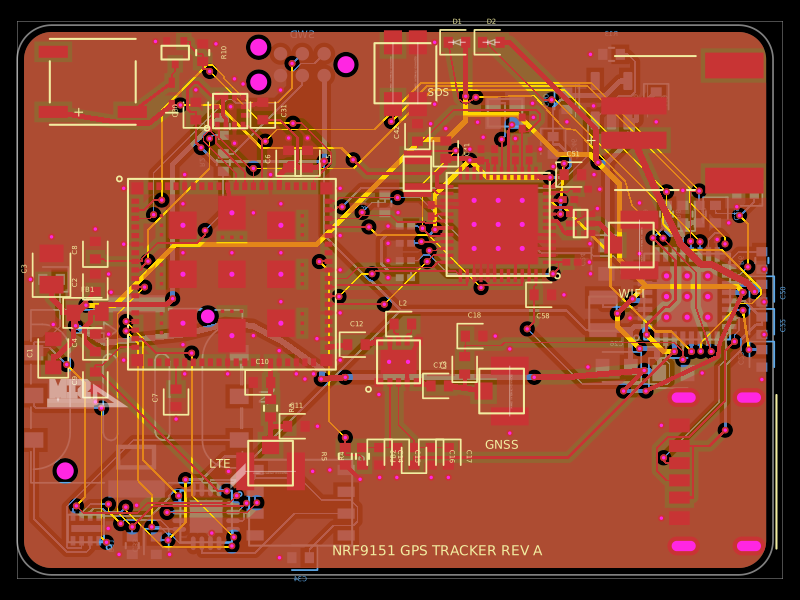 More from this authorpixalynx/nrf9151-gps-trackerA compact 44×32 mm, 4-layer nRF9151 LTE-M/NB-IoT/GNSS tracker PCB with nPM1300 LiPo/USB-C power, nano-SIM/eSIM switching, nRF7002 Wi‑Fi scanning, accelerometer, antennas, buzzer, LEDs, SOS button, and SWD/debug connectors.
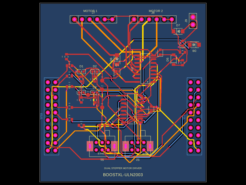 Similar packageabse/boostxl-uln2003This code defines a React component that models a through-hole or surface-mount LED with specified pin labels, footprint, silkscreen, and 3D CAD model for PCB layout.
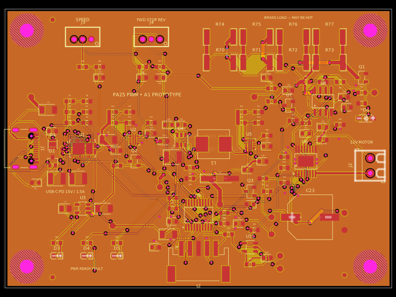 Discover something newAnasSarkiz/usb-c-pwm-pa25A component library defining an AO3400A N-channel MOSFET, 47 µF polarized capacitor, 3-pin through-hole connector, and 9.1 V Zener diode with PCB footprints and 3D CAD models.