pixalynx/pixal-nfc-card
This code defines React components representing specific electronic hardware components—namely, a 100-ohm SMD resistor, a surface-mount LED, and a chip with labeled pins—each modeled with detailed footprints, 3D CAD models, and manufacturer part information for PCB design.
- Version
- 1.1.0
- License
- unset
- Stars
- 0
dist/index.js
import { jsx, jsxs } from 'react/jsx-runtime';
import { Fragment } from 'react';

const pinLabels = {
    pin1: ["NC3"],
    pin2: ["NC1"],
    pin3: ["AC0"],
    pin4: ["AC1"],
    pin5: ["NC2"]
};
const pinAttributes = {
    pin1: { doNotConnect: true },
    pin2: { doNotConnect: true },
    pin5: { doNotConnect: true }
};
const ST25TN01K_AFH5 = (props) => {
    return (jsx("chip", { pinLabels: pinLabels, pinAttributes: pinAttributes, schHeight: 0.6, schPinArrangement: { leftSide: { pins: [3, 4], direction: "top-to-bottom" }, rightSide: { pins: [1, 2, 5], direction: "top-to-bottom" } }, supplierPartNumbers: {
            "jlcpcb": [
                "C3303589"
            ]
        }, manufacturerPartNumber: "ST25TN01K-AFH5", footprint: jsxs("footprint", { children: [jsx("smtpad", { portHints: ["pin2"], pcbX: "0mm", pcbY: "0mm", width: "0.2mm", height: "1.6mm", shape: "rect", solderPasteMargin: 0 }), jsx("smtpad", { portHints: ["pin5"], pcbX: "-0.4mm", pcbY: "0.5mm", width: "0.2mm", height: "0.6mm", shape: "rect", solderPasteMargin: 0 }), jsx("smtpad", { portHints: ["pin4"], pcbX: "0.4mm", pcbY: "0.5mm", width: "0.2mm", height: "0.6mm", shape: "rect", solderPasteMargin: 0 }), jsx("smtpad", { portHints: ["pin3"], pcbX: "0.4mm", pcbY: "-0.5mm", width: "0.2mm", height: "0.6mm", shape: "rect", solderPasteMargin: 0 }), jsx("smtpad", { portHints: ["pin1"], pcbX: "-0.4mm", pcbY: "-0.5mm", width: "0.2mm", height: "0.6mm", shape: "rect", solderPasteMargin: 0 }), jsx("silkscreencircle", { pcbX: "-0.65mm", pcbY: "-1.55mm", radius: "0.2mm", strokeWidth: "0.15mm" }), jsx("courtyardoutline", { outline: [{ "x": -1.0120000000000573, "y": 1.2659999999999627 }, { "x": 1.0119999999999436, "y": 1.2659999999999627 }, { "x": 1.0119999999999436, "y": -1.774000000000001 }, { "x": -1.0120000000000573, "y": -1.774000000000001 }, { "x": -1.0120000000000573, "y": 1.2659999999999627 }] })] }), cadModel: {
            objUrl: "https://modelcdn.tscircuit.com/easyeda_models/assets/C3303589.obj?uuid=189ea70a213f482e9891f9d83f16ed14",
            stepUrl: "https://modelcdn.tscircuit.com/easyeda_models/assets/C3303589.step?uuid=189ea70a213f482e9891f9d83f16ed14",
            pcbRotationOffset: 90,
            modelOriginPosition: { x: 0.00013969999997698324, y: 0, z: -0.01 },
        }, ...props }));
};

const r4$1 = (p) => ({ x: Math.round(p.x * 1e4) / 1e4, y: Math.round(p.y * 1e4) / 1e4 });
/** Closed polyline of a rounded rectangle centred on (cx, cy). */
function roundedRectPolyline(cx, cy, w, h, r, cornerSegments = 12) {
    const hw = w / 2 - r;
    const hh = h / 2 - r;
    const corners = [
        { x: cx + hw, y: cy + hh, a0: 0 },
        { x: cx - hw, y: cy + hh, a0: 90 },
        { x: cx - hw, y: cy - hh, a0: 180 },
        { x: cx + hw, y: cy - hh, a0: 270 },
    ];
    const pts = [];
    for (const c of corners) {
        for (let i = 0; i <= cornerSegments; i++) {
            const a = ((c.a0 + (90 * i) / cornerSegments) * Math.PI) / 180;
            pts.push({ x: c.x + r * Math.cos(a), y: c.y + r * Math.sin(a) });
        }
    }
    pts.push(pts[0]);
    return pts;
}
/** Cut a polyline into dashes of `dash` mm separated by `gap` mm. */
function dashPolyline(poly, dash, gap) {
    const dashes = [];
    let cur = [];
    let drawing = true;
    let remaining = dash;
    for (let i = 0; i < poly.length - 1; i++) {
        let a = poly[i];
        const b = poly[i + 1];
        let segLen = Math.hypot(b.x - a.x, b.y - a.y);
        while (segLen > 1e-9) {
            const step = Math.min(remaining, segLen);
            const t = step / segLen;
            const p = { x: a.x + (b.x - a.x) * t, y: a.y + (b.y - a.y) * t };
            if (drawing) {
                if (cur.length === 0)
                    cur.push(a);
                cur.push(p);
            }
            remaining -= step;
            segLen -= step;
            a = p;
            if (remaining <= 1e-9) {
                if (drawing && cur.length > 1)
                    dashes.push(cur);
                cur = [];
                drawing = !drawing;
                remaining = drawing ? dash : gap;
            }
        }
    }
    if (drawing && cur.length > 1)
        dashes.push(cur);
    return dashes.map((d) => d.map(r4$1));
}
/** Arc polyline around (cx, cy), angles in degrees counter-clockwise from +x. */
function arc(cx, cy, r, startDeg, endDeg, segments = 16) {
    const pts = [];
    for (let i = 0; i <= segments; i++) {
        const a = ((startDeg + ((endDeg - startDeg) * i) / segments) * Math.PI) / 180;
        pts.push(r4$1({ x: cx + r * Math.cos(a), y: cy + r * Math.sin(a) }));
    }
    return pts;
}

const r4 = (v) => Math.round(v * 1e4) / 1e4;
const coilPitch = (s) => s.width + s.gap;
/**
 * Rectangular spiral centreline from the outer terminal (right edge, below
 * centre) to the inner terminal (innermost right edge, above centre). Each turn
 * steps inward by one pitch at the bottom-right corner, so no copper crosses on
 * this layer and both terminals face the chip.
 */
function coilPath(s) {
    const p = coilPitch(s);
    const ym = (s.top + s.bottom) / 2;
    const pts = [{ x: s.right, y: ym - s.leadOffset }];
    for (let k = 0; k < s.turns; k++) {
        pts.push({ x: s.right - k * p, y: s.top - k * p }, { x: s.left + k * p, y: s.top - k * p }, { x: s.left + k * p, y: s.bottom + k * p }, { x: s.right - (k + 1) * p, y: s.bottom + k * p });
    }
    pts.push({ x: s.right - s.turns * p, y: ym + s.leadOffset });
    return pts.map((q) => ({ x: r4(q.x), y: r4(q.y) }));
}

const MU0_4PI = 1e-7;
/** Antiderivative for the mutual inductance of two parallel filaments at spacing d (metres). */
const H = (u, d) => u * Math.asinh(u / d) - Math.hypot(u, d);
/**
 * Greenhouse-style estimate for an axis-aligned printed coil: the self
 * inductance of every flat segment plus the signed mutual inductance of every
 * parallel pair (perpendicular pairs contribute nothing). Lengths in mm,
 * result in henries. Ignores parasitic capacitance, the chip's input model and
 * the LED load, so treat it as a starting point for tuning, not a measurement.
 */
function estimateInductance(path, widthMm, copperMm = 0.035) {
    const k = 1e-3;
    const segs = path.slice(1).map((b, i) => [path[i], b]);
    const wt = (widthMm + copperMm) * k;
    let L = 0;
    for (let i = 0; i < segs.length; i++) {
        const [a, b] = segs[i];
        const l = Math.hypot(b.x - a.x, b.y - a.y) * k;
        if (l === 0)
            continue;
        L += 2 * MU0_4PI * l * (Math.log((2 * l) / wt) + 0.5 + (0.2235 * wt) / l);
        const horizA = a.y === b.y;
        for (let j = i + 1; j < segs.length; j++) {
            const [c, e] = segs[j];
            if ((c.y === e.y) !== horizA)
                continue;
            const d = (horizA ? Math.abs(a.y - c.y) : Math.abs(a.x - c.x)) * k;
            if (d === 0)
                continue;
            const [a1, a2] = horizA ? [a.x, b.x] : [a.y, b.y];
            const [b1, b2] = horizA ? [c.x, e.x] : [c.y, e.y];
            const sign = Math.sign(a2 - a1) * Math.sign(b2 - b1);
            const [lo1, hi1] = [Math.min(a1, a2) * k, Math.max(a1, a2) * k];
            const [lo2, hi2] = [Math.min(b1, b2) * k, Math.max(b1, b2) * k];
            L += 2 * sign * MU0_4PI * (H(hi1 - lo2, d) - H(hi1 - hi2, d) - H(lo1 - lo2, d) + H(lo1 - hi2, d));
        }
    }
    return L;
}

/** ISO/IEC 7810 ID-1 (credit card) outline, centred on the board origin */
const CARD = { width: 85.6, height: 54, cornerRadius: 3.18, thickness: 0.6 };
/** Bottom antenna: nominal 2.54 uH with 50 pF IC capacitance gives ~14.1 MHz.
 * This is an estimate, not a tuning result. Qualify resonance in the final
 * nonmetallic stack; see docs/RF-VALIDATION.md before production release. */
const COIL = {
    left: -39.3,
    right: 6.7,
    bottom: -22,
    top: 22,
    turns: 5,
    width: 0.45,
    gap: 0.45,
    leadOffset: 3,
};
/** Top-side parts, placed just right of the coil terminals */
const PARTS = {
    // rotated 180 so AC0/AC1 (pins 3/4) face the coil
    U1: { x: 13.5, y: 0, rot: 180 },
};
const LEAD_WIDTH = 0.25;
const TERMINAL = { outerDiameter: 0.8, holeDiameter: 0.3 };

// Front print -- edit before ordering
const OWNER = "PIXALYNX";
const TAGLINE = "NFC CARD";
const coil = coilPath(COIL);
const outerEnd = coil[0];
const innerEnd = coil[coil.length - 1];
const coilMicrohenries = (estimateInductance(coil, COIL.width) * 1e6).toFixed(2);
// The coil is a DC short between its terminals. Core honours this for every
// component, but InductorProps does not declare it yet.
const coilTerminalsBonded = { internallyConnectedPins: [["pin1", "pin2"]] };
const coilCopperMargin = Math.max(COIL.width, TERMINAL.outerDiameter) / 2 + 0.25;
const courtyard = [
    { x: COIL.left - coilCopperMargin, y: COIL.bottom - coilCopperMargin },
    { x: COIL.right + coilCopperMargin, y: COIL.bottom - coilCopperMargin },
    { x: COIL.right + coilCopperMargin, y: COIL.top + coilCopperMargin },
    { x: COIL.left - coilCopperMargin, y: COIL.top + coilCopperMargin },
    { x: COIL.left - coilCopperMargin, y: COIL.bottom - coilCopperMargin },
];
// Front artwork: dashed tap zone just outside the coil, contactless icon, owner block on the right
const zone = { cx: (COIL.left + COIL.right) / 2, w: COIL.right - COIL.left + 2, h: COIL.top - COIL.bottom + 2 };
const zoneDashes = dashPolyline(roundedRectPolyline(zone.cx, 0, zone.w, zone.h, 4), 1, 0.8);
const icon = { x: zone.cx - 3, y: 7 };
const iconArcs = [2.2, 3.9, 5.6].map((r) => arc(icon.x, icon.y, r, -48, 48));
const iconDot = arc(icon.x, icon.y, 0.3, 0, 360, 12);
const textX = 28;
var index_circuit = () => (jsx("board", { title: "pixal-nfc-card", width: `${CARD.width}mm`, height: `${CARD.height}mm`, borderRadius: `${CARD.cornerRadius}mm`, thickness: `${CARD.thickness}mm`, layers: 2, solderMaskColor: "black", silkscreenColor: "white", children: jsxs("schematicsheet", { name: "NFC", displayName: "Passive NFC \u2014 revision B", sheetWidth: 60, sheetHeight: 40, children: [jsx("keepout", { shape: "rect", pcbX: zone.cx, pcbY: 0, width: 49, height: 47, layers: ["top", "bottom"], excludeRefs: [".L1"] }), jsx(ST25TN01K_AFH5, { name: "U1", pcbX: PARTS.U1.x, pcbY: PARTS.U1.y, pcbRotation: PARTS.U1.rot, schX: 0, schY: 0 }), jsx("inductor", { name: "L1", inductance: `${coilMicrohenries}uH`, doNotPlace: true, ...coilTerminalsBonded, pcbX: 0, pcbY: 0, schX: -3.2, schY: -1.2, schOrientation: "horizontal", footprint: jsxs("footprint", { children: [jsx("platedhole", { portHints: ["pin1"], shape: "circle", outerDiameter: `${TERMINAL.outerDiameter}mm`, holeDiameter: `${TERMINAL.holeDiameter}mm`, pcbX: outerEnd.x, pcbY: outerEnd.y }), jsx("platedhole", { portHints: ["pin2"], shape: "circle", outerDiameter: `${TERMINAL.outerDiameter}mm`, holeDiameter: `${TERMINAL.holeDiameter}mm`, pcbX: innerEnd.x, pcbY: innerEnd.y }), jsx("pcbtrace", { layer: "bottom", thickness: `${COIL.width}mm`, route: coil.map((p) => ({ route_type: "wire", x: p.x, y: p.y, width: COIL.width, layer: "bottom" })) }), jsx("courtyardoutline", { outline: courtyard })] }) }), jsx("trace", { name: "ANT_A", schDisplayLabel: "ANT_A", from: ".L1 > .pin2", to: ".U1 > .AC0", thickness: LEAD_WIDTH, pcbPath: [
                    { x: 11.7, y: 3 }, { x: 11.7, y: 1.1 }, { x: 12.3, y: 0.5 },
                ] }), jsx("trace", { name: "ANT_B", schDisplayLabel: "ANT_B", from: ".L1 > .pin1", to: ".U1 > .AC1", thickness: LEAD_WIDTH, pcbPath: [
                    { x: 11.7, y: -3 }, { x: 11.7, y: -1.1 }, { x: 12.3, y: -0.5 },
                ] }), zoneDashes.map((route, i) => (jsx(Fragment, { children: jsx("silkscreenpath", { route: route, strokeWidth: "0.3mm" }) }, `zone-${i}`))), iconArcs.map((route, i) => (jsx(Fragment, { children: jsx("silkscreenpath", { route: route, strokeWidth: "0.55mm" }) }, `icon-${i}`))), jsx("silkscreenpath", { route: iconDot, strokeWidth: "0.6mm" }), jsx("silkscreentext", { text: "TAP HERE", fontSize: "3.2mm", anchorAlignment: "center", pcbX: zone.cx, pcbY: -2.5 }), jsx("silkscreentext", { text: "HOLD PHONE HERE", fontSize: "1.7mm", anchorAlignment: "center", pcbX: zone.cx, pcbY: -6.5 }), jsx("silkscreentext", { text: OWNER, fontSize: "3.2mm", anchorAlignment: "center", pcbX: textX, pcbY: 15 }), jsx("silkscreentext", { text: TAGLINE, fontSize: "1.8mm", anchorAlignment: "center", pcbX: textX, pcbY: 10.5 }), jsx("silkscreenpath", { route: [{ x: 17, y: 8 }, { x: 40, y: 8 }], strokeWidth: "0.2mm" }), jsx("silkscreentext", { text: "TAP TO OPEN", fontSize: "1.7mm", anchorAlignment: "center", pcbX: textX, pcbY: 5 }), jsx("silkscreentext", { text: "MY PAGE", fontSize: "1.7mm", anchorAlignment: "center", pcbX: textX, pcbY: 2 }), jsx("silkscreentext", { text: "U1", fontSize: "1.7mm", anchorAlignment: "center", pcbX: 13.5, pcbY: -3.5 }), jsx("silkscreentext", { text: "13.56 MHz", fontSize: "1.7mm", anchorAlignment: "center", pcbX: textX, pcbY: -19 }), jsx("silkscreentext", { text: "REV B / NFC", fontSize: "1.7mm", anchorAlignment: "center", pcbX: textX, pcbY: -22 })] }) }));

export { index_circuit as default };
Related Packages
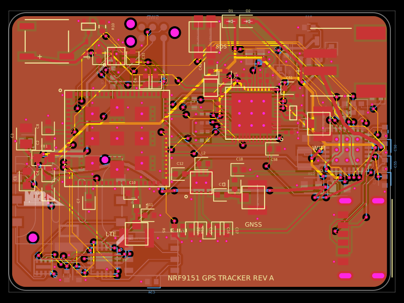 More from this authorpixalynx/nrf9151-gps-trackerA compact 44×32 mm, 4-layer nRF9151 LTE-M/NB-IoT/GNSS tracker PCB with nPM1300 LiPo/USB-C power, nano-SIM/eSIM switching, nRF7002 Wi‑Fi scanning, accelerometer, antennas, buzzer, LEDs, SOS button, and SWD/debug connectors.
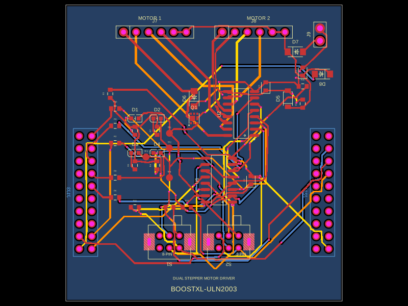 Similar packageabse/boostxl-uln2003This code defines a React component that models a through-hole or surface-mount LED with specified pin labels, footprint, silkscreen, and 3D CAD model for PCB layout.
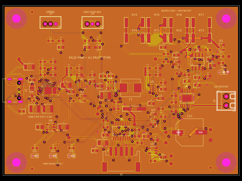 Discover something newAnasSarkiz/usb-c-pwm-pa25A component library defining an AO3400A N-channel MOSFET, 47 µF polarized capacitor, 3-pin through-hole connector, and 9.1 V Zener diode with PCB footprints and 3D CAD models.