pixalynx/pixal-nfc-card
This code defines React components representing specific electronic hardware components—namely, a 100-ohm SMD resistor, a surface-mount LED, and a chip with labeled pins—each modeled with detailed footprints, 3D CAD models, and manufacturer part information for PCB design.
- Version
- 1.1.0
- License
- unset
- Stars
- 0
README.md
# PIXALYNX NFC card — revision B

Passive 13.56 MHz ST25TN01K-AFH5 tag, printed five-turn antenna, 85.6 × 54 mm rounded outline, two copper layers and 0.6 mm FR-4. U1 is the only placed part. The experimental resistor/LED branch has been removed to avoid loading and rectifying the antenna voltage.

AC0 (pin 3) connects to the inner coil terminal; AC1 (pin 4) connects to the outer terminal. NC pins 1, 2 and 5 are electrically isolated. There is no battery, VCC or ground connection. The loop and the IC's internal nominal 50 pF tuning capacitance form the resonant circuit. Winding inductance is estimated at 2.536 µH; assembled RF performance remains unmeasured.

## Manufacturing status

**CAM review / prototype candidate, not production qualified.** Obtain JLCPCB acceptance of the 0.20 mm IC lands, stencil, 0.6 mm Standard-assembly panel/handling and placement orientation. Secure exact-part stock before committing to assembly. Qualify resonance/read range with physical samples before production.

- [Fabrication, assembly, sourcing and panel specification](docs/FABRICATION.md)
- [Factory panel proposal](docs/PANELIZATION.svg) — single-unit Gerbers must be panelized by the factory
- [RF and functional validation plan](docs/RF-VALIDATION.md)
- [Mechanical envelope and handling tests](docs/MECHANICAL.md)
- [Independent revision B re-review](docs/REV-B-REVIEW.md)

## Reproducible workflow

Requires Bun, Python 3 and uv on PATH. Dependencies are pinned in package.json/bun.lock; the geometry audit uses pinned Shapely 2.1.2 and Pillow 12.3.0 through uv.

```sh
bun install --frozen-lockfile
bun run dev
bun run fab
```

`bun run fab` typechecks and builds, audits the coil and actual Gerber geometry, checks connectivity/placement, removes only the four known unwanted plated-hole paste circles, and writes explicit BOM/CPL with U1 only. It includes regression checks for paste shrinkage, DNP mistakes, unknown paste and unwanted copper. The export aborts on failed release checks and removes the previous candidate ZIP before starting.

Use `fabrication/rev-b/pixal-nfc-card-rev-b-CAM-REVIEW.zip`. It includes single-unit Gerbers, drill, BOM/CPL, normalized Circuit JSON, drawings/instructions, logs, previews and SHA256 manifest. **Do not order from raw `tsci export`: the installed exporter adds antenna paste and L1 placement.** No node_modules have been patched. Source preview paste differs from released paste only at the two antenna holes; the normalizer records and verifies this intentional correction.

Both-layer keepout covers x=-40.8..8.2, y=-23.5..23.5 mm. L1 is explicitly exempt; only the two antenna feeds and two terminal lands may cross the region. Independent output-geometry checks enforce the intended copper population and coil turn clearances, including same-net conductors that ordinary DRC may miss.

Expected diagnostics: U1 has no requires_power/requires_ground pin because it is an RF-powered two-terminal tag. Bitmap short checking labels the two coil-to-terminal junctions as shorts; these are intended joins, accepted only at those locations with independent winding and connectivity checks. See re-review for exact dispositions. Never blanket-ignore a new warning or short.

The unused legacy LED/resistor import files are retained for history and are not instantiated or exported. The Everlight LED manufacturer's numbering is pin 1 anode, pin 2 cathode; the old README's cathode statement was wrong. These parts are not an approved alternate revision B population.
Related Packages
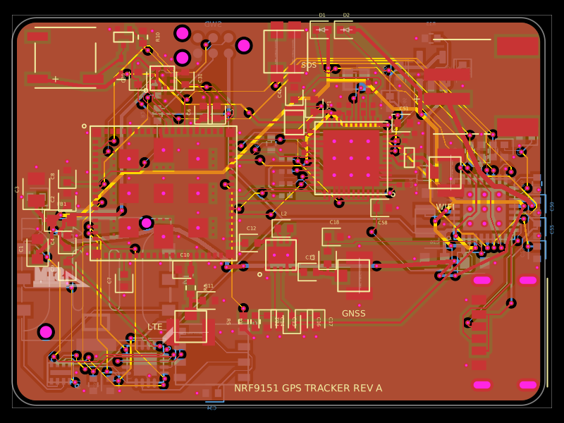 More from this authorpixalynx/nrf9151-gps-trackerA compact 44×32 mm, 4-layer nRF9151 LTE-M/NB-IoT/GNSS tracker PCB with nPM1300 LiPo/USB-C power, nano-SIM/eSIM switching, nRF7002 Wi‑Fi scanning, accelerometer, antennas, buzzer, LEDs, SOS button, and SWD/debug connectors.
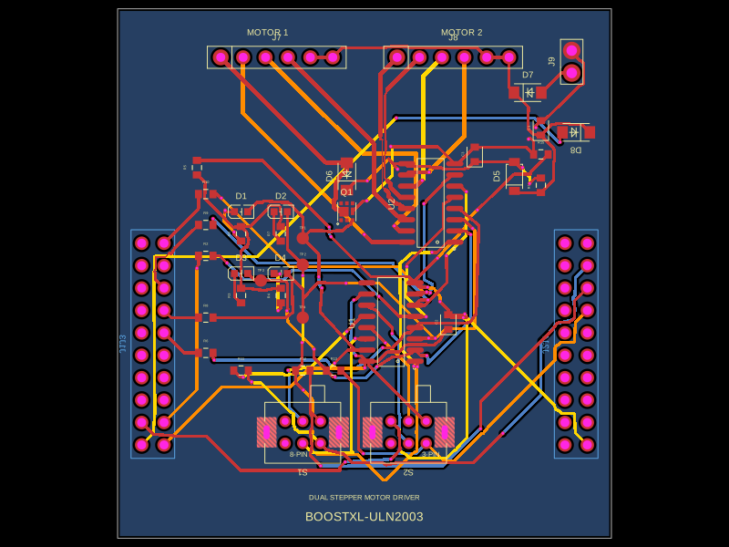 Similar packageabse/boostxl-uln2003This code defines a React component that models a through-hole or surface-mount LED with specified pin labels, footprint, silkscreen, and 3D CAD model for PCB layout.
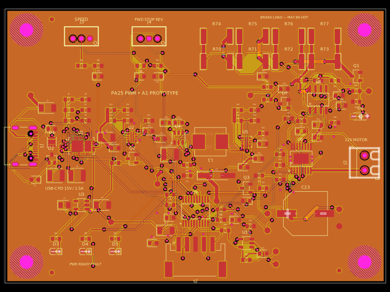 Discover something newAnasSarkiz/usb-c-pwm-pa25A component library defining an AO3400A N-channel MOSFET, 47 µF polarized capacitor, 3-pin through-hole connector, and 9.1 V Zener diode with PCB footprints and 3D CAD models.