pixalynx/pixal-gps
These files define two separate printed circuit boards: a small, two-layer battery cartridge with protection circuitry and contact pads for a pouch cell, and a larger, two-layer wireless charging dock featuring USB-C input, a resonant coil, and wireless power transmission components.
- Version
- 0.1.2
- License
- unset
- Stars
- 0
tracker.circuit.tsx
import { Fragment } from "react"
import { nrf9151GndPins, Nrf9151 } from "./parts/Nrf9151"
import { Npm1300 } from "./parts/Npm1300"
import { Bq51013b } from "./parts/Bq51013b"
import { Lis2dw12 } from "./parts/Lis2dw12"
import { NanoSimSocket } from "./parts/NanoSimSocket"
import { Sky65943, Tpd3f303, TactSwitch } from "./parts/RfFrontEnd"
import { Ufl, PogoPin, Contact } from "./parts/Connectors"
import { Cap, Res, Ind, Bead, type PassiveSpec } from "./lib/passives"
import { localPath } from "./lib/geometry"
import { Ind0806 } from "./lib/footprints"
import { GndMeshTraces, type GndMesh } from "./lib/gnd-mesh"
import { RoutedTraces, type RoutedLegs } from "./lib/routed-traces"
import routesJson from "./routing/tracker-routes.json"
import gndMeshJson from "./routing/tracker-gnd.json"

/**
 * PIXAL GPS tracker, PCB A (Rev A). 32 x 24 mm, 4 layers (JLC04161H-7628).
 *
 * Top: nRF9151 SiP, its VDD/VDD_GPIO/DEC0 decoupling, LTE pi-match + U.FL, GNSS LNA
 *      (SKY65943-11) + U.FL with optional active-antenna bias-T, AUX single-antenna jumper,
 *      status LEDs, SHPHLD button.
 * Bottom: nano-SIM socket + TPD3F303 SIM filter, nPM1300 PMIC + BUCK1 (1.8 V), BQ51013B
 *      Qi receiver + resonant/comm/clamp caps and coil pads, LIS2DW12 accelerometer,
 *      four battery-cartridge spring contacts, 2 x 5 pogo test/programming pads.
 *
 * Sources for every value: docs/sources.md and docs/design-report.md.
 */

export const BOARD = { w: 34, h: 24 }
const U1 = { x: -4.5, y: 1.0 } // SiP centre (top view)

// nRF9151 land positions in board coordinates (footprint constants, rotation 0).
export const sipPin = (n: number): { x: number; y: number } => {
  if (n === 1) return { x: U1.x - 5.5, y: U1.y + 5 }
  if (n >= 2 && n <= 19) return { x: U1.x - 5.625, y: U1.y + 4.25 - (n - 2) * 0.5 }
  if (n === 20) return { x: U1.x - 5.5, y: U1.y - 5 }
  if (n >= 21 && n <= 40) return { x: U1.x - 4.75 + (n - 21) * 0.5, y: U1.y - 5.125 }
  if (n === 41) return { x: U1.x + 5.5, y: U1.y - 5 }
  if (n >= 42 && n <= 59) return { x: U1.x + 5.625, y: U1.y - 4.25 + (n - 42) * 0.5 }
  if (n === 60) return { x: U1.x + 5.5, y: U1.y + 5 }
  if (n >= 61 && n <= 80) return { x: U1.x + 4.75 - (n - 61) * 0.5, y: U1.y + 5.125 }
  throw new Error(`no perimeter pin ${n}`)
}

// Schematic section origins (schematic units).
const S = {
  SIP: [0, 0], RF: [16, -2], SIM: [-18, -6], PWR: [0, -30], QI: [18, -30], MOTION: [18, 8], BAT: [-18, 8], DEBUG: [-18, 16], UI: [18, 16],
} as const
const sch = (sec: keyof typeof S, dx: number, dy: number): [number, number] => [S[sec][0] + dx, S[sec][1] + dy]

// ---------------------------------------------------------------------------------------
// Passive tables (positions are board coordinates in top view; bottom parts are mirrored by core)
// ---------------------------------------------------------------------------------------
const caps: PassiveSpec[] = [
  // nRF9151 VDD input filter (Nordic reference BOM v1.1): C3 47u, C4 10u before FB1; C1, C2 1u after it
  { name: "C1", value: "1uF", x: -12.45, y: -3.0, rot: 90, sch: sch("SIP", -9, 2), section: "SIP", note: "VDD HF, after FB1" },
  { name: "C2", value: "1uF", x: -12.45, y: 0.5, rot: 90, sch: sch("SIP", -9, 0), section: "SIP", note: "VDD HF, after FB1" },
  { name: "C3", value: "47uF", footprint: "0805", x: -15.0, y: 1.3, rot: 90, sch: sch("SIP", -13, 2), section: "SIP", note: "VDD bulk, X5R 10 V" },
  { name: "C4", value: "10uF", footprint: "0603", x: -14.9, y: -3.6, rot: 90, sch: sch("SIP", -13, 0), section: "SIP", note: "VDD bulk" },
  { name: "C5", value: "100nF", x: -0.1, y: 7.7, rot: 90, sch: sch("SIP", -5, 8), section: "SIP", note: "VDD_GPIO HF" },
  { name: "C6", value: "4.7uF", x: -1.2, y: 7.7, rot: 90, sch: sch("SIP", -7, 8), section: "SIP", note: "VDD_GPIO, X5R 6.3 V" },
  { name: "C7", value: "4.7uF", x: -7.75, y: -6.2, rot: 90, sch: sch("SIP", -9, -4), section: "SIP", note: "DEC0: exactly 4.7 uF (Nordic)" },
  { name: "C8", value: "100nF", x: -12.45, y: 2.4, rot: 90, sch: sch("SIP", -9, 4), section: "SIP", note: "nRESET bypass adjacent to pin 9" },
  { name: "C9", value: "100nF", x: -12.45, y: -5.2, rot: 90, sch: sch("SIP", -9, -2), section: "SIP", note: "SIM_1V8 supply cap (HDG 100-220 nF)" },
  // LTE matching reservation: shunt (DNP) - series 0R - shunt (DNP), placed on the ANT line
  { name: "C10", value: "22pF", x: -2.75, y: -5.3, rot: 0, sch: sch("RF", 2, 6), section: "RF", dnp: true, note: "LTE match shunt, DNP" },
  { name: "C11", value: "22pF", x: -0.75, y: -7.85, rot: 0, sch: sch("RF", 6, 6), section: "RF", dnp: true, note: "LTE match shunt, DNP" },
  // GNSS front end (SKY65943-11 + Nordic DK values)
  { name: "C12", value: "39pF", x: 2.75, y: -3.1, rot: 0, sch: sch("RF", 6, -2), section: "RF", note: "LNA out DC block to GPS pin" },
  { name: "C13", value: "39pF", x: 7.6, y: -5.5, rot: 0, sch: sch("RF", 12, 0), section: "RF", note: "GNSS antenna DC block" },
  { name: "C14", value: "100nF", x: 4.1, y: -9.6, rot: 270, sch: sch("RF", 4, -6), section: "RF", note: "LNA VEN filter" },
  { name: "C15", value: "100pF", x: 5.1, y: -9.6, rot: 270, sch: sch("RF", 6, -6), section: "RF", note: "LNA VEN filter" },
  { name: "C16", value: "100nF", x: 7.1, y: -9.6, rot: 270, sch: sch("RF", 10, -6), section: "RF", note: "LNA VCC" },
  { name: "C17", value: "100pF", x: 8.1, y: -9.6, rot: 270, sch: sch("RF", 12, -6), section: "RF", note: "LNA VCC" },
  { name: "C18", value: "39pF", x: -1.25, y: -5.7, rot: 90, sch: sch("RF", 0, 2), section: "RF", note: "AUX loop-back DC block (single-antenna option)" },
  // nPM1300 (Nordic reference config 1 minus BUCK2/LDO2)
  { name: "C20", value: "2.2uF", footprint: "0603", x: 2.4, y: 3.2, rot: 90, side: "bottom", sch: sch("PWR", -8, -2), section: "PWR", note: "VBAT, X7R 16 V" },
  { name: "C21", value: "10uF", footprint: "0603", x: 2.1, y: 6.2, rot: 270, side: "bottom", sch: sch("PWR", -8, 0), section: "PWR", note: "VSYS" },
  { name: "C22", value: "1uF", x: 0.8, y: 8.2, rot: 90, side: "bottom", sch: sch("PWR", -8, 2), section: "PWR", note: "VBUS" },
  { name: "C23", value: "1uF", x: 3.9, y: 7.8, rot: 90, sch: sch("PWR", -8, 4), section: "PWR", note: "VBUSOUT (mandatory even if unused)" },
  { name: "C24", value: "10uF", footprint: "0603", x: 10.9, y: 5.75, rot: 180, side: "bottom", sch: sch("PWR", 8, 0), section: "PWR", note: "PVDD (BUCK1 input) at the pin" },
  { name: "C25", value: "10uF", footprint: "0603", x: 11.8, y: 3.7, rot: 0, side: "bottom", sch: sch("PWR", 8, 2), section: "PWR", note: "VSYS/PVDD second cap" },
  { name: "C26", value: "10uF", footprint: "0603", x: 13.9, y: 7.4, rot: 0, side: "bottom", sch: sch("PWR", 10, -2), section: "PWR", note: "VOUT1 1.8 V" },
  { name: "C27", value: "100nF", x: 7.6, y: -1.3, rot: 90, side: "bottom", sch: sch("PWR", 0, -6), section: "PWR", note: "VDDIO" },
  { name: "C28", value: "100pF", x: 1.7, y: 0.7, rot: 90, side: "bottom", sch: sch("PWR", -10, -2), section: "PWR", note: "NTC pin (<=100 pF allowed)" },
  { name: "C29", value: "1uF", x: 9.6, y: -2.6, rot: 0, sch: sch("PWR", 4, 6), section: "PWR", note: "top side next to L3 (VANT is a load-switch rail; LDO-mode use would want this cap back at LSOUT1). LSOUT1 load-switch output (antenna bias)" },
  // BQ51013B (TI reference BOM)
  { name: "C30", value: "10nF", x: 15.9, y: 2.0, rot: 270, side: "bottom", sch: sch("QI", -6, 6), section: "QI", note: "BOOT1-AC1" },
  { name: "C31", value: "470nF", footprint: "0603", x: 15.9, y: -0.5, rot: 90, side: "bottom", sch: sch("QI", -6, 4), section: "QI", note: "CLAMP1-AC1, 25 V" },
  { name: "C32", value: "22nF", footprint: "0603", x: 15.9, y: -3.5, rot: 90, side: "bottom", sch: sch("QI", -6, 2), section: "QI", note: "COMM1-AC1, 50 V" },
  { name: "C33", value: "10nF", x: 8.2, y: 1.0, rot: 270, side: "bottom", sch: sch("QI", -6, -2), section: "QI", note: "BOOT2-AC2" },
  { name: "C34", value: "470nF", footprint: "0603", x: 8.85, y: -1.45, rot: 90, side: "bottom", sch: sch("QI", -6, -4), section: "QI", note: "CLAMP2-AC2, 25 V" },
  { name: "C35", value: "22nF", footprint: "0603", x: 9.0, y: -4.5, rot: 90, side: "bottom", sch: sch("QI", -6, -6), section: "QI", note: "COMM2-AC2, 50 V" },
  { name: "C36", value: "100nF", footprint: "0603", x: 14.9, y: 9.5, rot: 0, side: "bottom", sch: sch("QI", -12, 8), section: "QI", note: "C1 series resonant part A (50 V X7R)" },
  { name: "C37", value: "56nF", footprint: "0603", x: 14.9, y: 11.0, rot: 0, side: "bottom", sch: sch("QI", -12, 6), section: "QI", note: "C1 series resonant part B (50 V X7R); C1 = 156 nF for Ls' = 16 uH" },
  { name: "C38", value: "2.2nF", x: 13.9, y: 5.0, rot: 0, side: "bottom", sch: sch("QI", -12, 4), section: "QI", note: "C2 parallel detection cap, C0G 50 V" },
  { name: "C39", value: "10uF", footprint: "0805", x: 5.2, y: -1.6, rot: 0, side: "bottom", sch: sch("QI", 6, 8), section: "QI", jlc: "C3039694", note: "RECT, X7R 25 V" },
  { name: "C40", value: "10uF", footprint: "0805", x: 7.2, y: -4.7, rot: 90, side: "bottom", sch: sch("QI", 8, 8), section: "QI", jlc: "C3039694", note: "RECT, X7R 25 V" },
  { name: "C41", value: "100nF", x: 3.0, y: -1.6, rot: 90, side: "bottom", sch: sch("QI", 10, 8), section: "QI", note: "RECT HF bypass" },
  { name: "C42", value: "10uF", footprint: "0603", x: 14.9, y: 3.7, rot: 0, side: "bottom", sch: sch("QI", 6, 2), section: "QI", note: "OUT (VBUS_QI)" },
  { name: "C43", value: "100nF", x: 15.9, y: 5.6, rot: 90, side: "bottom", sch: sch("QI", 8, 2), section: "QI", note: "OUT HF bypass" },
  // LIS2DW12
  { name: "C44", value: "100nF", x: -3.0, y: 7.6, rot: 90, side: "bottom", sch: sch("MOTION", -4, 2), section: "MOTION", note: "VDD_IO" },
  { name: "C45", value: "10uF", x: -4.0, y: 7.6, rot: 90, side: "bottom", sch: sch("MOTION", -6, 2), section: "MOTION", note: "VDD" },
  // SIM socket VCC at the socket
  { name: "C46", value: "10nF", x: -15.6, y: -9.8, rot: 90, side: "bottom", sch: sch("SIM", 4, -4), section: "SIM", note: "SIM VCC at the socket (DK C48)" },
]
const ress: PassiveSpec[] = [
  { name: "R1", value: "10k", x: -5.0, y: 9.6, rot: 90, side: "bottom", sch: sch("SIP", -5, 4), section: "SIP", note: "ENABLE to VDD (Nordic R1)" },
  { name: "R2", value: "1k", x: -5.0, y: 7.5, rot: 90, side: "bottom", sch: sch("SIP", -5, 2), section: "SIP", note: "nRESET series (Nordic R2)" },
  { name: "R3", value: "0", x: -2.25, y: -6.8, rot: 90, sch: sch("RF", 4, 6), section: "RF", note: "LTE match series element (0R for a 50 ohm connector)" },
  { name: "R4", value: "1k", x: 3.1, y: -9.6, rot: 90, sch: sch("RF", 2, -6), section: "RF", note: "COEX0 -> LNA VEN series" },
  { name: "R5", value: "100k", x: 2.1, y: -9.6, rot: 270, sch: sch("RF", 0, -6), section: "RF", note: "COEX0 pull-down (mandatory, Nordic)" },
  { name: "R6", value: "0", x: 6.0, y: -6.7, rot: 90, sch: sch("RF", 2, 2), section: "RF", dnp: true, note: "AUX -> LNA input jumper: fit for single-antenna mode (%XANTCFG)" },
  { name: "R7", value: "100k", x: -7.6, y: 7.7, rot: 90, sch: sch("BAT", 4, 4), section: "BAT", note: "BAT_ID pull-up driven from P0.14 (only during measurement)" },
  { name: "R8", value: "100k", x: -6.5, y: 7.7, rot: 90, sch: sch("BAT", 6, 4), section: "BAT", note: "BAT_ID series protection into AIN0" },
  { name: "R9", value: "47k", x: 4.0, y: 0.4, rot: 90, side: "bottom", sch: sch("PWR", -6, -6), section: "PWR", note: "VSET1 = 1.8 V" },
  { name: "R10", value: "10k", x: 6.6, y: 0.4, rot: 90, side: "bottom", sch: sch("PWR", -2, -6), section: "PWR", note: "I2C SDA pull-up" },
  { name: "R11", value: "10k", x: 5.6, y: 0.4, rot: 90, side: "bottom", sch: sch("PWR", -4, -6), section: "PWR", note: "I2C SCL pull-up" },
  { name: "R12", value: "68", x: 12.9, y: -5.6, rot: 0, side: "bottom", sch: sch("QI", 6, -4), section: "QI", note: "R1: ILIM = R1 + RFOD = 268 ohm -> IMAX 1 A" },
  { name: "R13", value: "200", x: 14.9, y: -6.8, rot: 0, side: "bottom", sch: sch("QI", 8, -4), section: "QI", note: "RFOD (TI default 196 ohm), calibrate" },
  { name: "R14", value: "20k", x: 12.9, y: -6.8, rot: 0, side: "bottom", sch: sch("QI", 10, -4), section: "QI", note: "ROS RECT->FOD (TI default), calibrate" },
  { name: "R15", value: "10k", x: 14.9, y: -5.6, rot: 0, side: "bottom", sch: sch("QI", 4, -4), section: "QI", note: "TS unused -> 10k to PGND" },
  { name: "R16", value: "100k", x: 14.1, y: -8.4, rot: 90, side: "bottom", sch: sch("QI", 10, 0), section: "QI", note: "CHG open-drain pull-up to 1V8" },
]
const inds: PassiveSpec[] = [
  { name: "L1", value: "2.2uH", footprint: <Ind0806 />, fpKey: "0806", x: 10.8, y: 7.6, rot: 180, side: "bottom", sch: sch("PWR", 6, -2), section: "PWR", note: "BUCK1, DFE201612E-2R2M (Isat 1.8 A)" },
  { name: "L2", value: "9.1nH", x: 5.45, y: -1.9, rot: 0, sch: sch("RF", 8, -4), section: "RF", note: "SKY65943 interstage (FILT_OUT-AMP_IN)" },
  { name: "L3", value: "68nH", x: 9.05, y: -4.3, rot: 90, sch: sch("RF", 14, 2), section: "RF", dnp: true, note: "Active-antenna bias-T inductor, DNP" },
]

// Test/programming pads (bottom, 2 x 5, 1.27 mm pitch) and battery contacts
const tpRowA = ["SWDIO", "SWDCLK", "RESET", "V1V8", "GND"] as const
const tpRowB = ["TX", "RX", "VSYS", "VBAT", "VBUS"] as const

/** Every land on the ground net (see the comment at the render site). */
const GND_LANDS = [
  ...nrf9151GndPins.map((p) => `U1.${p}`),
  "U2.GND1", "U2.GND2", "U2.GND3", "U2.GND4", "U2.GND_PAD",
  "U3.PVSS1", "U3.PVSS2", "U3.AVSS", "U3.VSET2", "U3.CC1", "U3.CC2", "U3.LSIN2", "U3.LSOUT2",
  "U4.GND", "U5.PGND1", "U5.PGND2", "U5.PGND", "U5.AD", "U6.GND1", "U6.GND2", "U6.SDO", "U6.RES",
  "J1.GND1", "J1.GND2", "J2.GND1", "J2.GND2", "J3.SHELL1", "J3.SHELL2", "J3.C5", "SW1.B", "SW1.B2", "P2.P", "TP5.P",
  "C1.pin2", "C2.pin2", "C3.pin2", "C4.pin2", "C5.pin2", "C6.pin2", "C7.pin1", "C8.pin2", "C9.pin1", "C10.pin1", "C11.pin2",
  "C14.pin2", "C15.pin2", "C16.pin2", "C17.pin2", "C20.pin2", "C21.pin2", "C22.pin2", "C23.pin2", "C24.pin2", "C25.pin2",
  "C26.pin2", "C27.pin2", "C28.pin2", "C29.pin2", "C39.pin2", "C40.pin2", "C41.pin2", "C42.pin2", "C43.pin2", "C44.pin2",
  "C45.pin2", "C46.pin2", "R5.pin2", "R9.pin2", "R13.pin2", "R15.pin2",
]

const routes = routesJson as RoutedLegs
// The signal/power copper is a local Freerouting pass imported as explicit legs (routing/tracker-routes.json,
// see docs/routing.md). The native autorouter is opt-in for experiments: PIXAL_AUTOROUTE=1 bunx tsci build ...
const nativeAutoroute = typeof process !== "undefined" && process.env?.PIXAL_AUTOROUTE === "1"

export default () => (
  <board width={BOARD.w} height={BOARD.h} layers={4} thickness={1.6} borderRadius={1} routingDisabled={!nativeAutoroute}
    title="PIXAL GPS tracker A / nRF9151 + nPM1300 / Rev A"
    fabricatorPreset="jlcpcb_standard"
    minTraceWidth={0.1} minTraceToPadEdgeClearance={0.1} minPadEdgeToPadEdgeClearance={0.1}
    minViaHoleDiameter={0.2} minViaPadDiameter={0.4} minBoardEdgeClearance={0.3}
    pcbStyle={{ viaHoleDiameter: "0.2mm", viaPadDiameter: "0.4mm" }}
    defaultTraceWidth={0.15} autorouterEffortLevel="10x" doubleSidedAssembly
  >
    <autoroutingphase minTraceToPadEdgeClearance="0.15mm" minViaEdgeToPadEdgeClearance="0.2mm" />

    {Object.keys(S).map((name) => <Fragment key={name}><schematicsection name={name} displayName={name} /></Fragment>)}

    <net name="GND" isGroundNet />
    <net name="VSYS" isPowerNet nominalTraceWidth={0.4} />
    <net name="VBAT" isPowerNet nominalTraceWidth={0.4} />
    <net name="VBUS_QI" isPowerNet nominalTraceWidth={0.3} />
    <net name="V1V8" isPowerNet nominalTraceWidth={0.25} />
    <net name="VDD_NRF" isPowerNet nominalTraceWidth={0.4} />

    {/* ----------------------------- nRF9151 SiP ----------------------------- */}
    <Nrf9151 name="U1" pcbX={U1.x} pcbY={U1.y} schX={S.SIP[0]} schY={S.SIP[1]} schSectionName="SIP" />
    <Bead name="FB1" value="22R" mpn="BLM18SD220SN1D" jlc="C710389" x={-12.9} y={-1.25} rot={0} sch={sch("SIP", -11, 1)} section="SIP" />
    <trace from="FB1.B" to="net.VDD_NRF" />
    <trace from="FB1.A" to="net.VSYS" />
    <trace from="U1.VDD" to="net.VDD_NRF" />
    <trace from="C1.pin1" to="net.VDD_NRF" />
    <trace from="C2.pin1" to="net.VDD_NRF" />
    <trace from="C3.pin1" to="net.VSYS" />
    <trace from="C4.pin1" to="net.VSYS" />
    <trace from="R1.pin1" to="net.VDD_NRF" /><trace from="R1.pin2" to="U1.ENABLE" />
    <trace from="U1.VDD_GPIO" to="net.V1V8" />
    <trace from="C5.pin1" to="net.V1V8" />
    <trace from="C6.pin1" to="net.V1V8" />
    <trace from="U1.DEC0" to="net.DEC0" /><trace from="C7.pin2" to="net.DEC0" />
    <trace from="U1.nRESET" to="net.NRESET" /><trace from="C8.pin1" to="net.NRESET" />
    <trace from="R2.pin2" to="net.NRESET" /><trace from="R2.pin1" to="net.RESET_TP" />
    <trace from="U1.SWDIO" to="net.SWDIO" /><trace from="U1.SWDCLK" to="net.SWDCLK" />
    {/* corner land: the nine centre GND lands carry vias and are internally bonded */}
    {/* SIM interface (class C 1.8 V) through the TPD3F303 EMI/ESD filter */}
    <trace from="U1.SIM_1V8" to="net.SIM_1V8" /><trace from="C9.pin2" to="net.SIM_1V8" />
    <trace from="U1.SIM_RST" to="U4.DATA1_IN" /><trace from="U1.SIM_CLK" to="U4.CLK_IN" /><trace from="U1.SIM_IO" to="U4.DATA2_IN" />
    {/* Debug UART for the console, exposed on pogo pads */}
    <trace from="U1.P0_26" to="net.UART_TX" /><trace from="U1.P0_27" to="net.UART_RX" />
    {/* I2C bus (TWIM) to nPM1300 and LIS2DW12 */}
    <trace from="U1.P0_28" to="net.I2C_SDA" /><trace from="U1.P0_29" to="net.I2C_SCL" />
    <trace from="U1.P0_30" to="net.PMIC_INT" />
    <trace from="U1.P0_31" to="net.ACC_INT1" /><trace from="U1.P0_00" to="net.ACC_INT2" />
    <trace from="U1.P0_01" to="net.QI_EN" /><trace from="U1.P0_02" to="net.QI_CHG" />
    {/* Battery ID: P0.14 drives the pull-up only while AIN0 samples, so it costs no sleep current */}
    <trace from="U1.P0_14" to="R7.pin1" /><trace from="R7.pin2" to="net.BAT_ID" />
    <trace from="R8.pin2" to="net.BAT_ID" /><trace from="R8.pin1" to="U1.P0_13" />

    {/* ----------------------------- LTE antenna path ----------------------------- */}
    <Ufl name="J1" pcbX={-2.25} pcbY={-10.0} pcbRotation={180} schX={S.RF[0] + 8} schY={S.RF[1] + 8} schSectionName="RF" />
    <trace name="rf_ant_1" from="U1.ANT" to="C10.pin2" thickness={0.32} pcbPath={[]} />
    <trace name="rf_ant_2" from="C10.pin2" to="R3.pin2" thickness={0.32} pcbPath={[]} />
    <trace name="rf_ant_3" from="R3.pin1" to="J1.SIG" thickness={0.32} pcbPath={[]} />
    <trace name="rf_ant_4" from="C11.pin1" to="R3.pin1" thickness={0.32} pcbPath={localPath([{ x: -2.25, y: -7.85 }], { x: -0.75, y: -7.85 }, 0)} />


    {/* ----------------------------- GNSS front end ----------------------------- */}
    <Sky65943 name="U2" pcbX={5.2} pcbY={-4.1} schX={S.RF[0] + 8} schY={S.RF[1] - 3} schSectionName="RF" />
    <Ufl name="J2" pcbX={11.2} pcbY={-5.8} pcbRotation={270} schX={S.RF[0] + 16} schY={S.RF[1]} schSectionName="RF" />
    <trace name="rf_gps_1" from="U1.GPS" to="C12.pin1" thickness={0.32} pcbPath={[]} />
    <trace name="rf_gps_2" from="C12.pin2" to="U2.RF_OUT" thickness={0.32} pcbPath={[]} />
    <trace from="U2.AMP_IN" to="L2.pin1" /><trace from="U2.FILT_OUT" to="L2.pin2" />
    <trace name="rf_gnss_in_1" from="U2.RF_IN" to="C13.pin1" thickness={0.32} pcbPath={[]} />
    <trace name="rf_gnss_in_2" from="C13.pin2" to="J2.SIG" thickness={0.32} pcbPath={[]} />
    {/* Active-antenna bias-T inductor (DNP): its pad hangs off the GNSS line as a 0.83 mm stub that ends exactly on the
        J2 -> C13 leg (the last segment repeats that copper), so the option costs no extra discontinuity when unfitted. */}
    <trace name="rf_bias_stub" from="L3.pin1" to="J2.SIG" thickness={0.25} pcbPath={localPath([{ x: 9.05, y: -5.638 }], { x: 9.05, y: -4.3 }, 90)} />
    <trace from="L3.pin2" to="net.VANT" />
    {/* LNA enable and supply cross under the AUX line on L3 (vias sit 0.34 mm clear of the 50-ohm copper; the router
        keepout is wider than the DRC needs, which is why these two are hand-routed), and the LNA's GND2/GND3 lands tie
        straight into the paddle. */}
    <trace name="lna_ven" from="U2.VEN" to="R4.pin2" thickness={0.15} pcbPath={localPath([{ x: 4.7, y: -6.0 }, { x: 4.7, y: -6.0, via: true, toLayer: "inner2" }, { x: 3.1, y: -8.0 }, { x: 3.1, y: -8.0, via: true, toLayer: "top" }], { x: 5.2, y: -4.1 }, 0)} />
    <trace name="lna_vcc" from="U2.VCC" to="C16.pin1" thickness={0.15} pcbPath={localPath([{ x: 5.2, y: -6.3 }, { x: 5.2, y: -6.3, via: true, toLayer: "inner2" }, { x: 7.1, y: -8.0 }, { x: 7.1, y: -8.0, via: true, toLayer: "top" }], { x: 5.2, y: -4.1 }, 0)} />
    <trace name="lna_gnd2" from="U2.GND2" to="U2.GND_PAD" thickness={0.25} pcbPath={localPath([{ x: 5.7, y: -4.6 }], { x: 5.2, y: -4.1 }, 0)} />
    {/* VSYS: LSIN1 and VOUT2 (same row of the PMIC) joined under the row on L3 so the router cannot park a via in
        the LSOUT1/LED escape lanes (it did, twice). */}
    <trace name="pmic_lsin1_vout2" from="U3.LSIN1" to="U3.VOUT2" thickness={0.2} pcbPath={localPath([{ x: 6.05, y: 8.6 }, { x: 6.05, y: 8.6, via: true, toLayer: "inner2" }, { x: 8.05, y: 8.75 }, { x: 8.05, y: 8.75, via: true, toLayer: "bottom" }], { x: 6.3, y: 5.0 }, 0)} />
    {/* VBUSOUT decoupling: the PMIC land faces C21 across a 0.85 mm gap; the leg steps into that gap on L4, drops a via
        beside the CC1 land and reaches C23 on the top side. */}
    <trace name="pmic_vbusout" from="U3.VBUSOUT" to="C23.pin1" thickness={0.15} pcbPath={localPath([{ x: 3.05, y: 5.75 }, { x: 3.05, y: 6.4 }, { x: 3.05, y: 6.4, via: true, toLayer: "top" }, { x: 3.5, y: 6.65 }], { x: 6.3, y: 5.0 }, 0)} />
    {/* Qi FOD node: leaves the receiver's left column on a via and runs on L3 down to the FOD resistor pair. */}
    <trace name="qi_fod" from="U5.FOD" to="R12.pin2" thickness={0.15} pcbPath={localPath([{ x: 9.8, y: -0.55 }, { x: 9.8, y: -0.55, via: true, toLayer: "inner2" }, { x: 11.7, y: -5.2 }, { x: 11.7, y: -5.2, via: true, toLayer: "bottom" }], { x: 12.3, y: 0.2 }, 0)} />
    <trace name="lna_gnd3" from="U2.GND3" to="U2.GND_PAD" thickness={0.25} pcbPath={localPath([{ x: 6.0, y: -3.6 }], { x: 5.2, y: -4.1 }, 0)} />

    {/* The last five connections Freerouting would not make after six attempts on this board (see
        docs/routing.md "What the router would not do"): found by a grid-search hand router
        (scripts/hand-route-net.py) on inner2, or a direct same-layer detour, or (for GND) a plane via. */}
    <trace name="hand_U1_P0_31" from="U1.P0_31" to="U6.INT1" thickness={0.15} pcbPath={[{ x: 5.625, y: -0.25 }, { x: 5.175, y: -0.25, via: true, toLayer: "inner2" }, { x: 5.3342, y: -0.05 }, { x: 5.3342, y: 0.05 }, { x: 5.4342, y: 0.15 }, { x: 5.4342, y: 0.25 }, { x: 5.6342, y: 0.45 }, { x: 5.7342, y: 0.45 }, { x: 6.1342, y: 0.85 }, { x: 6.6342, y: 0.85 }, { x: 6.7342, y: 0.95 }, { x: 7.8342, y: 0.95 }, { x: 9.3342, y: -0.55 }, { x: 10.1342, y: -0.55 }, { x: 10.8342, y: 0.15 }, { x: 10.8342, y: 0.25 }, { x: 10.9342, y: 0.35 }, { x: 10.9342, y: 1.95 }, { x: 10.2342, y: 2.65 }, { x: 10.2342, y: 2.95 }, { x: 9.9342, y: 3.25 }, { x: 9.8342, y: 3.25 }, { x: 9.7342, y: 3.35 }, { x: 8.8342, y: 3.35 }, { x: 8.3342, y: 2.85 }, { x: 8.3342, y: 2.75 }, { x: 7.4342, y: 1.85 }, { x: 7.3342, y: 1.85 }, { x: 7.2342, y: 1.75 }, { x: 4.7342, y: 1.75 }, { x: 3.1342, y: 3.35 }, { x: 3.0342, y: 3.35 }, { x: 2.4342, y: 3.95 }, { x: 2.4342, y: 5.35 }, { x: 2.6342, y: 5.55 }, { x: 2.6342, y: 5.65 }, { x: 2.7342, y: 5.75 }, { x: 2.7342, y: 6.05 }, { x: 2.5342, y: 6.2408, via: true, toLayer: "top" }, { x: 0.625, y: 8.15 }]} />
    <trace name="hand_U3_VBUS" from="U3.VBUS" to="C22.pin1" thickness={0.15} pcbPath={[{ x: -2.451, y: 0.25 }, { x: -2.151, y: 0.25, via: true, toLayer: "inner2" }, { x: -2.1121, y: 1.05 }, { x: -2.7121, y: 1.65 }, { x: -2.7121, y: 3.95 }, { x: -3.2121, y: 4.45 }, { x: -3.3121, y: 4.45 }, { x: -3.4121, y: 4.55 }, { x: -4.6121, y: 4.55 }, { x: -4.7121, y: 4.45 }, { x: -5.2121, y: 4.45 }, { x: -5.7121, y: 3.9221, via: true, toLayer: "bottom" }, { x: -5.5, y: 3.71 }]} />
    <trace name="hand_U6_SCL" from="U6.SCL" to="U1.P0_29" thickness={0.15} pcbPath={[{ x: -0.75, y: -0.875 }, { x: -0.3193, y: -4.1468, via: true, toLayer: "inner2" }, { x: 0.1807, y: -4.65 }, { x: 0.1807, y: -4.95 }, { x: 0.5807, y: -5.35 }, { x: 0.5807, y: -5.75 }, { x: 1.7807, y: -6.95 }, { x: 1.7807, y: -8.15 }, { x: 1.8807, y: -8.25 }, { x: 1.8807, y: -8.35 }, { x: 2.4807, y: -8.95 }, { x: 3.0807, y: -8.95 }, { x: 3.825, y: -9.65, via: true, toLayer: "top" }, { x: 4.125, y: -9.65 }]} />
    <trace name="hand_R13_pin1" from="R13.pin1" to="R14.pin2" thickness={0.15} pcbPath={[{ x: 0.49, y: -0.0 }, { x: 0.29, y: -0.2 }, { x: 0.19, y: -0.2 }, { x: -0.21, y: -0.6 }, { x: -0.81, y: -0.6 }, { x: -1.01, y: -0.4 }, { x: -1.01, y: 0.4 }, { x: -1.21, y: 0.6 }, { x: -1.91, y: 0.6 }, { x: -2.51, y: -0.0 }]} />
    <trace name="hand_C41_pin2" from="C41.pin2" to="net.GND" thickness={0.25} pcbPath={[{ x: -0.51, y: -0.0 }, { x: -0.6514, y: 0.1414, via: true, toLayer: "inner1" }]} />

    {/* LNA enable from COEX0 (modem drives it high while GNSS receives); 100k pull-down mandatory */}
    <trace from="U1.COEX0" to="net.COEX0" /><trace from="R5.pin1" to="net.COEX0" />
    <trace from="R4.pin1" to="net.COEX0" /><trace from="R4.pin2" to="net.LNA_VEN" />
    <trace from="U2.VEN" to="net.LNA_VEN" /><trace from="C14.pin1" to="net.LNA_VEN" />
    <trace from="C15.pin1" to="net.LNA_VEN" />
    <Bead name="FB2" value="120R" mpn="BLM15AG121SN1D" jlc="C85812" footprint="0402" x={6.1} y={-9.6} rot={90} sch={sch("RF", 8, -6)} section="RF" />
    <trace from="FB2.A" to="net.V1V8" /><trace from="FB2.B" to="net.LNA_VCC" />
    <trace from="U2.VCC" to="net.LNA_VCC" /><trace from="C16.pin1" to="net.LNA_VCC" />
    <trace from="C17.pin1" to="net.LNA_VCC" />
    {/* Single-antenna option: ANT -> internal switch -> AUX -> (C18, R6) -> LNA input */}
    <trace name="rf_aux_1" from="U1.AUX" to="C18.pin2" thickness={0.32} pcbPath={[]} />
    <trace name="rf_aux_2" from="C18.pin1" to="R6.pin1" thickness={0.32}
      pcbPath={localPath([{ x: -1.25, y: -7.0 }, { x: 5.6, y: -7.0 }], { x: -1.25, y: -5.7 }, 90)} />
    <trace name="rf_aux_3" from="R6.pin2" to="U2.RF_IN" thickness={0.32} pcbPath={[]} />

    {/* ----------------------------- SIM ----------------------------- */}
    <NanoSimSocket name="J3" pcbX={-9.3} pcbY={-2.5} pcbRotation={270} layer="bottom" schX={S.SIM[0]} schY={S.SIM[1]} schSectionName="SIM" />
    <Tpd3f303 name="U4" pcbX={-13.0} pcbY={-9.9} layer="bottom" schX={S.SIM[0] + 6} schY={S.SIM[1]} schSectionName="SIM" />
    <trace from="U4.DATA1_OUT" to="J3.RST" /><trace from="U4.CLK_OUT" to="J3.CLK" /><trace from="U4.DATA2_OUT" to="J3.IO" />
    <trace from="U4.VCC" to="net.SIM_1V8" /><trace from="J3.VCC" to="net.SIM_1V8" /><trace from="C46.pin1" to="net.SIM_1V8" />


    {/* ----------------------------- nPM1300 power management ----------------------------- */}
    <Npm1300 name="U3" pcbX={6.3} pcbY={5.0} layer="bottom" schX={S.PWR[0]} schY={S.PWR[1]} schSectionName="PWR" />
    <trace from="U3.VBAT" to="net.VBAT" /><trace from="C20.pin1" to="net.VBAT" />
    <trace from="U3.VSYS" to="net.VSYS" /><trace from="C21.pin1" to="net.VSYS" />
    <trace from="U3.PVDD" to="net.VSYS" /><trace from="C24.pin1" to="net.VSYS" />
    <trace from="C25.pin1" to="net.VSYS" />
    <trace from="U3.VBUS" to="net.VBUS_QI" /><trace from="C22.pin1" to="net.VBUS_QI" />
    <trace from="U3.VBUSOUT" to="net.VBUSOUT" /><trace from="C23.pin1" to="net.VBUSOUT" />

    <trace from="U3.SW1" to="L1.pin2" /><trace from="L1.pin1" to="net.V1V8" /><trace from="U3.VOUT1" to="net.V1V8" />
    <trace from="C26.pin1" to="net.V1V8" />
    {/* AVSS paddle (with vias) is bonded to PVSS1/2 in the part */}
    <trace from="U3.VSET1" to="R9.pin1" />
    <trace from="U3.VOUT2" to="net.VSYS" />

    <trace from="U3.LSIN1" to="net.VSYS" /><trace from="U3.LSOUT1" to="net.VANT" /><trace from="C29.pin1" to="net.VANT" />
    {/* Every ground land is declared here (the generated mesh / router JSON only add copper geometry).
        Internally-bonded groups do not propagate net membership to their other pins, so each pin is listed.
        VSET2 -> GND disables BUCK2 (Nordic config 3); CC1/CC2 grounded (no USB-C); BQ51013B AD unused -> GND;
        LIS2DW12 SDO/SA0 -> GND = address 0x18, RES -> GND per ST. */}
    {GND_LANDS.map((p) => <Fragment key={`gnd-${p}`}><trace from={p} to="net.GND" /></Fragment>)}
    <trace from="U3.VDDIO" to="net.V1V8" /><trace from="C27.pin1" to="net.V1V8" />
    <trace from="U3.SDA" to="net.I2C_SDA" /><trace from="U3.SCL" to="net.I2C_SCL" />
    <trace from="R10.pin1" to="net.I2C_SDA" /><trace from="R10.pin2" to="net.V1V8" />
    <trace from="R11.pin1" to="net.I2C_SCL" /><trace from="R11.pin2" to="net.V1V8" />
    <trace from="U3.GPIO0" to="net.PMIC_INT" />
    <trace from="U3.NTC" to="net.BAT_NTC" /><trace from="C28.pin1" to="net.BAT_NTC" />
    <trace from="U3.SHPHLD" to="net.SHPHLD" />

    {/* Status LEDs on the nPM1300 5 mA constant-current sinks (no series resistors) */}
    <led name="D1" footprint="0402" color="green" pcbX={7.8} pcbY={10.8} schX={S.UI[0]} schY={S.UI[1]} schSectionName="UI" supplierPartNumbers={{ jlcpcb: ["C688877"] }} />
    <led name="D2" footprint="0402" color="red" pcbX={9.9} pcbY={10.8} schX={S.UI[0] + 3} schY={S.UI[1]} schSectionName="UI" supplierPartNumbers={{ jlcpcb: ["C779449"] }} />
    <trace from="D1.anode" to="net.VSYS" /><trace from="D1.cathode" to="U3.LED1" />
    <trace from="D2.anode" to="net.VSYS" /><trace from="D2.cathode" to="U3.LED2" />
    <TactSwitch name="SW1" pcbX={13.6} pcbY={8.6} schX={S.UI[0] + 6} schY={S.UI[1]} schSectionName="UI" />
    <trace from="SW1.A" to="net.SHPHLD" />

    {/* ----------------------------- Qi receiver ----------------------------- */}
    <Bq51013b name="U5" pcbX={12.3} pcbY={0.2} layer="bottom" schX={S.QI[0]} schY={S.QI[1]} schSectionName="QI" />
    <Contact name="P5" diameter={1.8} pcbX={11.6} pcbY={10.6} layer="bottom" schX={S.QI[0] - 16} schY={S.QI[1] + 8} schSectionName="QI" />
    <Contact name="P6" diameter={1.8} pcbX={9.6} pcbY={10.2} layer="bottom" schX={S.QI[0] - 16} schY={S.QI[1] + 4} schSectionName="QI" />
    <trace from="P5.P" to="net.COIL1" /><trace from="C36.pin2" to="net.COIL1" /><trace from="C37.pin2" to="net.COIL1" />
    <trace from="C36.pin1" to="net.AC1" /><trace from="C37.pin1" to="net.AC1" /><trace from="U5.AC1" to="net.AC1" />
    <trace from="P6.P" to="net.AC2" /><trace from="U5.AC2" to="net.AC2" />
    <trace from="C38.pin1" to="net.AC1" /><trace from="C38.pin2" to="net.AC2" />
    <trace from="U5.BOOT1" to="net.QI_BOOT1" /><trace from="C30.pin1" to="net.QI_BOOT1" /><trace from="C30.pin2" to="net.AC1" />
    <trace from="U5.CLAMP1" to="net.QI_CLAMP1" /><trace from="C31.pin1" to="net.QI_CLAMP1" /><trace from="C31.pin2" to="net.AC1" />
    <trace from="U5.COMM1" to="net.QI_COMM1" /><trace from="C32.pin1" to="net.QI_COMM1" /><trace from="C32.pin2" to="net.AC1" />
    <trace from="U5.BOOT2" to="net.QI_BOOT2" /><trace from="C33.pin1" to="net.QI_BOOT2" /><trace from="C33.pin2" to="net.AC2" />
    <trace from="U5.CLAMP2" to="net.QI_CLAMP2" /><trace from="C34.pin1" to="net.QI_CLAMP2" /><trace from="C34.pin2" to="net.AC2" />
    <trace from="U5.COMM2" to="net.QI_COMM2" /><trace from="C35.pin1" to="net.QI_COMM2" /><trace from="C35.pin2" to="net.AC2" />
    <trace from="U5.RECT" to="net.RECT" /><trace from="C39.pin1" to="net.RECT" />
    <trace from="C40.pin1" to="net.RECT" /><trace from="C41.pin1" to="net.RECT" />
    <trace from="U5.OUT" to="net.VBUS_QI" /><trace from="C42.pin1" to="net.VBUS_QI" />
    <trace from="C43.pin1" to="net.VBUS_QI" />
    <trace from="U5.ILIM" to="R12.pin1" /><trace from="R12.pin2" to="net.QI_FOD" /><trace from="U5.FOD" to="net.QI_FOD" />
    <trace from="R13.pin1" to="net.QI_FOD" />
    <trace from="R14.pin1" to="net.RECT" /><trace from="R14.pin2" to="net.QI_FOD" />
    <trace from="U5.TS_CTRL" to="R15.pin1" />

    <trace from="U5.EN1" to="net.QI_EN" /><trace from="U5.EN2" to="net.QI_EN" />
    <trace from="U5.CHG" to="net.QI_CHG" /><trace from="R16.pin1" to="net.QI_CHG" /><trace from="R16.pin2" to="net.V1V8" />
    {/* the paddle PGND carries vias; PGND1/2 are the routed lands */}

    {/* ----------------------------- Accelerometer ----------------------------- */}
    <Lis2dw12 name="U6" pcbX={-3.0} pcbY={9.4} schX={S.MOTION[0]} schY={S.MOTION[1]} schSectionName="MOTION" />
    <trace from="U6.VDD" to="net.V1V8" /><trace from="U6.VDD_IO" to="net.V1V8" /><trace from="U6.CS" to="net.V1V8" />

    <trace from="U6.SCL" to="net.I2C_SCL" /><trace from="U6.SDA" to="net.I2C_SDA" />
    <trace from="U6.INT1" to="net.ACC_INT1" /><trace from="U6.INT2" to="net.ACC_INT2" />
    <trace from="C44.pin1" to="net.V1V8" />
    <trace from="C45.pin1" to="net.V1V8" />

    {/* ----------------------------- Battery cartridge contacts ----------------------------- */}
    {/* Order BAT+, GND, NTC, ID: a 180-degree reversed cartridge never applies reverse polarity */}
    <PogoPin name="P1" pcbX={-3.0} pcbY={10.5} layer="bottom" schX={S.BAT[0]} schY={S.BAT[1] + 3} schSectionName="BAT" />
    <PogoPin name="P2" pcbX={0.0} pcbY={10.5} layer="bottom" schX={S.BAT[0]} schY={S.BAT[1] + 1} schSectionName="BAT" />
    <PogoPin name="P3" pcbX={3.0} pcbY={10.5} layer="bottom" schX={S.BAT[0]} schY={S.BAT[1] - 1} schSectionName="BAT" />
    <PogoPin name="P4" pcbX={6.0} pcbY={10.5} layer="bottom" schX={S.BAT[0]} schY={S.BAT[1] - 3} schSectionName="BAT" />
    <trace from="P1.P" to="net.VBAT" /><trace from="P3.P" to="net.BAT_NTC" /><trace from="P4.P" to="net.BAT_ID" />

    {/* ----------------------------- Programming / test pads ----------------------------- */}
    {tpRowA.map((n, i) => (
      <Fragment key={n}>
        <Contact name={`TP${i + 1}`} diameter={1.0} pcbX={-9.0 + (i - 2) * 1.27} pcbY={9.235} layer="bottom" schX={S.DEBUG[0] + i * 2} schY={S.DEBUG[1] + 2} schSectionName="DEBUG" />
        <trace from={`TP${i + 1}.P`} to={n === "GND" ? "net.GND" : n === "RESET" ? "net.RESET_TP" : `net.${n}`} />
      </Fragment>
    ))}
    {tpRowB.map((n, i) => (
      <Fragment key={n}>
        <Contact name={`TP${i + 6}`} diameter={1.0} pcbX={-9.0 + (i - 2) * 1.27} pcbY={7.965} layer="bottom" schX={S.DEBUG[0] + i * 2} schY={S.DEBUG[1]} schSectionName="DEBUG" />
        <trace from={`TP${i + 6}.P`} to={n === "TX" ? "net.UART_TX" : n === "RX" ? "net.UART_RX" : n === "VBUS" ? "net.VBUS_QI" : `net.${n}`} />
      </Fragment>
    ))}

    {/* ----------------------------- passives ----------------------------- */}
    {caps.map((c) => <Cap key={c.name} {...c} />)}
    {ress.map((r) => <Res key={r.name} {...r} />)}
    {inds.map((l) => <Ind key={l.name} {...l} />)}

    {/* Ground: generated stub-to-plane vias and same-layer links (routing/tracker-gnd.json) */}
    <GndMeshTraces mesh={gndMeshJson as GndMesh} />
    {/* Signal and power copper: Freerouting session imported as land-to-land legs (routing/tracker-routes.json) */}
    <RoutedTraces routes={routes} />

    {/* ----------------------------- copper ----------------------------- */}
    <copperpour name="GND_L1" layer="top" connectsTo="net.GND" clearance={0.25} boardEdgeMargin={0.4} />
    <copperpour name="GND_L2" layer="inner1" connectsTo="net.GND" clearance={0.25} boardEdgeMargin={0.4} unbroken />
    <copperpour name="GND_L4" layer="bottom" connectsTo="net.GND" clearance={0.25} boardEdgeMargin={0.4} />

    <silkscreentext text="PIXAL GPS A / REV A" pcbX={9} pcbY={11.2} fontSize={0.8} anchorAlignment="center" />
    <silkscreentext text="LTE" pcbX={-5.2} pcbY={-10.0} fontSize={0.7} anchorAlignment="center" />
    <silkscreentext text="GNSS" pcbX={14.3} pcbY={-4.0} fontSize={0.7} anchorAlignment="center" />
    <silkscreentext text="BAT+  GND  NTC  ID" pcbX={1.5} pcbY={8.9} fontSize={0.6} anchorAlignment="center" layer="bottom" />
    <silkscreentext text="COIL" pcbX={11.3} pcbY={9.0} fontSize={0.6} anchorAlignment="center" layer="bottom" />
  </board>
)
Related Packages
 More from this authorpixalynx/esp32-gps-cellular-trackerThis code defines a hardware layout comprising a Wi-Fi-enabled ESP32 module, GPS module, cellular GSM module, battery management components (including charger, protection circuits, and voltage regulators), USB-C connector, SIM card holder, RF components, and supporting passive components for a comprehensive GPS+Cellular tracker device.
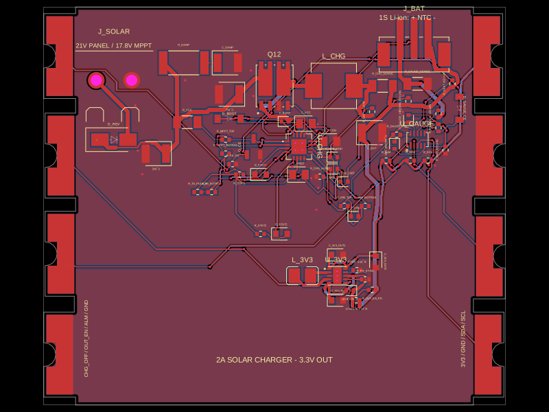 Similar packageShiboSoftwareDev/solar-battery-charger-moduleThis hardware setup integrates a solar panel, a lithium-ion battery, and a multi-rail buck converter with a battery charging IC, protection circuitry, and monitoring components, enabling solar power harvesting, battery charging, and power distribution in an embedded system.
 Discover something newimrishabh18/fitness_watchThis circuit integrates an ESP-12E microcontroller with various sensors and peripherals, including a AO3400A MOSFET for switching loads, to enable wireless control and sensor data processing.