pixalynx/pixal-gps
These files define two separate printed circuit boards: a small, two-layer battery cartridge with protection circuitry and contact pads for a pouch cell, and a larger, two-layer wireless charging dock featuring USB-C input, a resonant coil, and wireless power transmission components.
- Version
- 0.1.2
- License
- unset
- Stars
- 0
review/source-build/parts/UsbC.tsx
import type { ConnectorProps } from "@tscircuit/props"

// USB-C 16-pin top-mount receptacle, JLCPCB basic part C2765186
// ("TYPE-C 16PIN 2MD(073)"). Geometry is a verbatim copy of the footprint
// the parts engine fetches for this part number (12 SMD contacts at
// 0.5mm pitch, four plated shell slots, two 0.7mm alignment-peg holes),
// with the pegs expressed only as NPTH holes. The fetched version also
// carries the pegs as pcb_cutouts, which the placement checker flags as
// the connector overlapping its own cutouts and that in turn suppresses
// autorouting -- so the footprint is spelled out here instead. Pin numbers
// follow tscircuit's canonical USB-C order so `standard="usb_c"` still
// drives the schematic symbol.
const pinLabels = {
  pin1: ["GND1"],
  pin2: ["VBUS1"],
  pin3: ["CC1"],
  pin4: ["DP1"],
  pin5: ["DM1", "DN1"],
  pin6: ["SBU1"],
  pin7: ["SBU2"],
  pin8: ["DM2", "DN2"],
  pin9: ["DP2"],
  pin10: ["CC2"],
  pin11: ["VBUS2"],
  pin12: ["GND2"],
  pin13: ["SHELL1"],
  pin14: ["SHELL2"],
  pin15: ["SHELL3"],
  pin16: ["SHELL4"],
} as const

const wide = { width: "0.55mm", height: "1.1mm", shape: "rect" as const }
const narrow = { width: "0.3mm", height: "1.1mm", shape: "rect" as const }

export const TYPE_C_16PIN_2MD_073 = (props: ConnectorProps) => {
  return (
    <connector
      standard="usb_c"
      pinLabels={pinLabels}
      manufacturerPartNumber="TYPE-C 16PIN 2MD(073)"
      supplierPartNumbers={{ jlcpcb: ["C2765186"] }}
      footprint={
        <footprint>
          {/* Contact row (rear of the receptacle) */}
          <smtpad portHints={["pin1"]} pcbX="-3.2mm" pcbY="2.125mm" {...wide} />
          <smtpad portHints={["pin2"]} pcbX="-2.4mm" pcbY="2.125mm" {...wide} />
          <smtpad portHints={["pin7"]} pcbX="-1.75mm" pcbY="2.125mm" {...narrow} />
          <smtpad portHints={["pin3"]} pcbX="-1.25mm" pcbY="2.125mm" {...narrow} />
          <smtpad portHints={["pin8"]} pcbX="-0.75mm" pcbY="2.125mm" {...narrow} />
          <smtpad portHints={["pin4"]} pcbX="-0.25mm" pcbY="2.125mm" {...narrow} />
          <smtpad portHints={["pin5"]} pcbX="0.25mm" pcbY="2.125mm" {...narrow} />
          <smtpad portHints={["pin9"]} pcbX="0.75mm" pcbY="2.125mm" {...narrow} />
          <smtpad portHints={["pin6"]} pcbX="1.25mm" pcbY="2.125mm" {...narrow} />
          <smtpad portHints={["pin10"]} pcbX="1.75mm" pcbY="2.125mm" {...narrow} />
          <smtpad portHints={["pin11"]} pcbX="2.4mm" pcbY="2.125mm" {...wide} />
          <smtpad portHints={["pin12"]} pcbX="3.2mm" pcbY="2.125mm" {...wide} />
          {/* Shell legs: rear pair and front pair */}
          <platedhole portHints={["pin13"]} shape="pill" pcbX="-4.325mm" pcbY="1.575mm" outerWidth="1.1mm" outerHeight="1.9mm" holeWidth="0.6mm" holeHeight="1.4mm" />
          <platedhole portHints={["pin14"]} shape="pill" pcbX="4.325mm" pcbY="1.575mm" outerWidth="1.1mm" outerHeight="1.9mm" holeWidth="0.6mm" holeHeight="1.4mm" />
          <platedhole portHints={["pin15"]} shape="pill" pcbX="-4.325mm" pcbY="-2.625mm" outerWidth="1.2mm" outerHeight="1.6mm" holeWidth="0.6mm" holeHeight="1.0mm" />
          <platedhole portHints={["pin16"]} shape="pill" pcbX="4.325mm" pcbY="-2.625mm" outerWidth="1.2mm" outerHeight="1.6mm" holeWidth="0.6mm" holeHeight="1.0mm" />
          {/* Alignment pegs (non-plated) */}
          <hole pcbX="-2.89mm" pcbY="1.055mm" diameter="0.7mm" />
          <hole pcbX="2.89mm" pcbY="1.055mm" diameter="0.7mm" />
          {/* Body outline: 8.94mm wide, 7.35mm deep from the contact row */}
          <silkscreenpath route={[{ x: 4.572, y: -1.647 }, { x: 4.572, y: 0.347 }]} />
          <silkscreenpath route={[{ x: 4.572, y: -5.076 }, { x: 4.572, y: -3.603 }]} />
          <silkscreenpath route={[{ x: -4.5, y: -1.644 }, { x: -4.5, y: 0.344 }]} />
          <silkscreenpath route={[{ x: -4.5, y: -5.225 }, { x: -4.5, y: -3.606 }]} />
          <silkscreenpath route={[{ x: 4.5, y: -5.225 }, { x: -4.5, y: -5.225 }]} />
          <silkscreentext text="{NAME}" pcbX="0mm" pcbY="3.6mm" anchorAlignment="center" fontSize="1mm" />
          <courtyardoutline outline={[{ x: -4.753, y: 2.934 }, { x: 4.815, y: 2.934 }, { x: 4.815, y: -5.491 }, { x: -4.753, y: -5.491 }, { x: -4.753, y: 2.934 }]} />
        </footprint>
      }
      cadModel={{
        objUrl: "https://modelcdn.tscircuit.com/easyeda_models/assets/C2765186.obj?uuid=4ee8413127e64716b804db03d4b340ae",
        stepUrl: "https://modelcdn.tscircuit.com/easyeda_models/assets/C2765186.step?uuid=4ee8413127e64716b804db03d4b340ae",
        pcbRotationOffset: 0,
        modelOriginPosition: { x: -0.0000127, y: 1.57499705, z: -1.6800018 },
      }}
      {...props}
    />
  )
}
Related Packages
 More from this authorpixalynx/esp32-gps-cellular-trackerThis code defines a hardware layout comprising a Wi-Fi-enabled ESP32 module, GPS module, cellular GSM module, battery management components (including charger, protection circuits, and voltage regulators), USB-C connector, SIM card holder, RF components, and supporting passive components for a comprehensive GPS+Cellular tracker device.
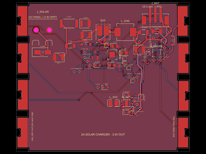 Similar packageShiboSoftwareDev/solar-battery-charger-moduleThis hardware setup integrates a solar panel, a lithium-ion battery, and a multi-rail buck converter with a battery charging IC, protection circuitry, and monitoring components, enabling solar power harvesting, battery charging, and power distribution in an embedded system.
 Discover something newimrishabh18/fitness_watchThis circuit integrates an ESP-12E microcontroller with various sensors and peripherals, including a AO3400A MOSFET for switching loads, to enable wireless control and sensor data processing.