pixalynx/pixal-gps
These files define two separate printed circuit boards: a small, two-layer battery cartridge with protection circuitry and contact pads for a pouch cell, and a larger, two-layer wireless charging dock featuring USB-C input, a resonant coil, and wireless power transmission components.
- Version
- 0.1.2
- License
- unset
- Stars
- 0
review/source-build/dock.circuit.tsx
import { Fragment } from "react"
import { Ip6829 } from "./parts/Ip6829"
import { TYPE_C_16PIN_2MD_073 as UsbC } from "./parts/UsbC"
import { Cap, Res, type PassiveSpec } from "./lib/passives"
import { pad, outline, courtyard } from "./lib/footprints"

/**
 * PIXAL GPS charging dock, board C (Rev A). 56 x 44 mm, 2 layers, 1.6 mm.
 *
 * USB-C 5 V in -> Injoinic IP6829 single-chip Qi BPP transmitter (integrated full bridge)
 * -> series resonant capacitor (4 x 100 nF C0G 100 V = 400 nF) -> WPC A11 coil (6.3 uH,
 * e.g. Vishay IWTX50R0CZEB6R3KF1 or CND-tek YX-A11-R500800-R0845, 50 mm ferrite-backed)
 * mounted above the PCB with its ferrite toward the board. Circuit follows the IP6829
 * datasheet V1.10 Figure 14 / BOM table exactly (docs/wireless-charging.md); no MCU, no
 * firmware work: two status LEDs, NTC input parked with 100 k, dynamic-FOD threshold 100 k.
 */
const CoilPad = () => (
  <footprint>
    {pad(1, 0, 0, 2.5, 3.5)}
    {outline(2.8, 3.8)}
    {courtyard(3.0, 4.0)}
  </footprint>
)
const U = { x: -6, y: 4 }
const caps: PassiveSpec[] = [
  { name: "C1", value: "10uF", footprint: "0805", x: -16, y: 12, rot: 90, sch: [-14, 6], section: "IN", note: "VIN bulk, 25 V" },
  { name: "C2", value: "22uF", footprint: "0805", x: -13.5, y: 12, rot: 90, sch: [-12, 6], section: "IN", note: "VIN bulk, 25 V" },
  { name: "C3", value: "22uF", footprint: "0805", x: -11, y: 12, rot: 90, sch: [-10, 6], section: "IN", note: "VIN bulk, 25 V" },
  { name: "C4", value: "100nF", x: -9, y: 12, rot: 90, sch: [-8, 6], section: "IN", note: "VIN HF" },
  { name: "C5", value: "2.2nF", x: 2.5, y: 9.5, rot: 90, sch: [8, 2], section: "SENSE", note: "VDET to GND: static FOD sensitivity" },
  { name: "C6", value: "100nF", x: 1.5, y: 3.5, rot: 90, sch: [8, -2], section: "TX", note: "BST2-LX2 bootstrap (must not be omitted)" },
  { name: "C7", value: "2.2uF", footprint: "0603", x: -12, y: 4, rot: 90, sch: [-8, 2], section: "IN", note: "VCC internal LDO" },
  { name: "C8", value: "100nF", x: 1.5, y: 0, rot: 90, sch: [8, -4], section: "TX", note: "BST1-LX1 bootstrap (must not be omitted)" },
  { name: "C9", value: "15nF", footprint: "0603", x: 9, y: 12, rot: 0, sch: [14, 4], section: "SENSE", note: "demodulator node to GND (ref C7)" },
  { name: "C10", value: "15nF", footprint: "0603", x: 6, y: 12, rot: 0, sch: [12, 6], section: "SENSE", note: "V_DECODE series (ref C10)" },
  { name: "C11", value: "100nF", footprint: "1206", x: 13, y: 0, rot: 90, sch: [16, -4], section: "TX", jlc: "C405303", note: "C0G 100 V, resonant 1/4" },
  { name: "C12", value: "100nF", footprint: "1206", x: 15.5, y: 0, rot: 90, sch: [18, -4], section: "TX", jlc: "C405303", note: "C0G 100 V, resonant 2/4" },
  { name: "C13", value: "100nF", footprint: "1206", x: 18, y: 0, rot: 90, sch: [20, -4], section: "TX", jlc: "C405303", note: "C0G 100 V, resonant 3/4" },
  { name: "C14", value: "100nF", footprint: "1206", x: 20.5, y: 0, rot: 90, sch: [22, -4], section: "TX", jlc: "C405303", note: "C0G 100 V, resonant 4/4 (400 nF for the 6.3 uH A11 coil)" },
  { name: "C15", value: "15nF", footprint: "0603", x: -12, y: -6, rot: 0, sch: [-8, -6], section: "SENSE", note: "NTC pin filter (ref C12)" },
]
const ress: PassiveSpec[] = [
  { name: "R1", value: "0", x: -9.5, y: -3.5, rot: 0, sch: [-4, -8], section: "SENSE", note: "ISENSE Kelvin lead (ref R2)" },
  { name: "R2", value: "0", x: -9.5, y: -5.0, rot: 0, sch: [-2, -8], section: "SENSE", note: "IGND Kelvin lead (ref R3)" },
  { name: "R3", value: "0.02", footprint: "0805", x: -9.5, y: -8.0, rot: 0, sch: [0, -8], section: "SENSE", jlc: "C601084", note: "20 mOhm 1 % current-sense (PGND to GND), 0.75 W" },
  { name: "R4", value: "3.3k", x: 9, y: 9.5, rot: 0, sch: [12, 2], section: "SENSE", note: "ref R22" },
  { name: "R5", value: "33k", x: 12, y: 12, rot: 0, sch: [14, 6], section: "SENSE", note: "ref R25" },
  { name: "R6", value: "100k", x: 5.5, y: 7.5, rot: 0, sch: [10, 0], section: "SENSE", note: "ref R20, VDET" },
  { name: "R7", value: "10k", x: 5.5, y: 5.5, rot: 0, sch: [10, -2], section: "SENSE", note: "ref R21, VDET" },
  { name: "R8", value: "100k", x: -13.8, y: -8, rot: 0, sch: [-8, -8], section: "SENSE", note: "LOSS_THR: dynamic FOD threshold (50-130 k)" },
  { name: "R9", value: "100k", x: -16.5, y: -4, rot: 0, sch: [-6, -6], section: "SENSE", note: "NTC unused: 100 k to GND (datasheet)" },
  { name: "R10", value: "1k", x: -4, y: -9, rot: 0, sch: [-4, -12], section: "UI", note: "LED1 series" },
  { name: "R11", value: "1k", x: 0, y: -9, rot: 0, sch: [0, -12], section: "UI", note: "LED2 series" },
]

export default () => (
  <board width={56} height={44} layers={2} thickness={1.6} borderRadius={2}
    title="PIXAL GPS charging dock C / Rev A"
    minTraceWidth={0.15} minTraceToPadEdgeClearance={0.15} minPadEdgeToPadEdgeClearance={0.15}
    minViaHoleDiameter={0.3} minViaPadDiameter={0.6} minBoardEdgeClearance={0.3}
    pcbStyle={{ viaHoleDiameter: "0.3mm", viaPadDiameter: "0.6mm" }} defaultTraceWidth={0.25} autorouterEffortLevel="5x"
  >
    <autoroutingphase minTraceToPadEdgeClearance="0.25mm" minViaEdgeToPadEdgeClearance="0.3mm" />
    {["IN", "TX", "SENSE", "UI"].map((n) => <Fragment key={n}><schematicsection name={n} displayName={n} /></Fragment>)}
    <net name="GND" isGroundNet />
    <net name="PGND" isPowerNet nominalTraceWidth={1.0} />
    <net name="VIN" isPowerNet nominalTraceWidth={0.8} />
    <net name="LX1" nominalTraceWidth={1.0} />
    <net name="LX2" nominalTraceWidth={1.0} />
    <net name="COIL_A" nominalTraceWidth={1.0} />

    <UsbC name="J1" pcbX={-21} pcbY={-6} pcbRotation={270} schX={-18} schY={0} schSectionName="IN" />
    <trace from="J1.VBUS1" to="net.VIN" /><trace from="J1.VBUS2" to="net.VIN" />
    <trace from="J1.GND1" to="net.GND" /><trace from="J1.GND2" to="net.GND" /><trace from="J1.SHELL1" to="net.GND" />
    <trace from="J1.CC1" to="net.USB_CC1" /><trace from="J1.CC2" to="net.USB_CC2" />
    <trace from="J1.DP1" to="net.USB_DP" /><trace from="J1.DP2" to="net.USB_DP" /><trace from="J1.DM1" to="net.USB_DM" /><trace from="J1.DM2" to="net.USB_DM" />

    <Ip6829 name="U1" pcbX={U.x} pcbY={U.y} schX={0} schY={0} schSectionName="TX" />
    <trace from="U1.VIN1" to="net.VIN" /><trace from="C1.pin1" to="net.VIN" /><trace from="C1.pin2" to="net.PGND" />
    <trace from="C2.pin1" to="net.VIN" /><trace from="C2.pin2" to="net.PGND" /><trace from="C3.pin1" to="net.VIN" /><trace from="C3.pin2" to="net.PGND" />
    <trace from="C4.pin1" to="net.VIN" /><trace from="C4.pin2" to="net.PGND" />
    <trace from="U1.VCC" to="net.VCC_LDO" /><trace from="C7.pin1" to="net.VCC_LDO" /><trace from="C7.pin2" to="net.GND" />
    <trace from="U1.CC1" to="net.USB_CC1" /><trace from="U1.CC2" to="net.USB_CC2" /><trace from="U1.DP" to="net.USB_DP" /><trace from="U1.DM" to="net.USB_DM" />
    <trace from="U1.GND" to="net.GND" /><trace from="U1.AGND" to="net.GND" />
    {/* Power ground returns through the 20 mOhm sense resistor; ISENSE/IGND are Kelvin leads */}
    <trace from="U1.PGND" to="net.PGND" /><trace from="R3.pin1" to="net.PGND" /><trace from="R3.pin2" to="net.GND" />
    <trace from="U1.ISENSE" to="R1.pin1" /><trace from="R1.pin2" to="net.PGND" />
    <trace from="U1.IGND" to="R2.pin1" /><trace from="R2.pin2" to="net.GND" />
    {/* Bridge outputs, bootstraps, resonant tank, coil */}
    <trace from="U1.LX1A" to="net.LX1" /><trace from="U1.LX2A" to="net.LX2" />
    <trace from="U1.BST1" to="net.BST1" /><trace from="C8.pin1" to="net.BST1" /><trace from="C8.pin2" to="net.LX1" />
    <trace from="U1.BST2" to="net.BST2" /><trace from="C6.pin1" to="net.BST2" /><trace from="C6.pin2" to="net.LX2" />
    {["C11", "C12", "C13", "C14"].map((c) => <Fragment key={c}><trace from={`${c}.pin1`} to="net.LX1" /><trace from={`${c}.pin2`} to="net.COIL_A" /></Fragment>)}
    <chip name="P1" footprint={<CoilPad />} pcbX={24} pcbY={6} pinLabels={{ pin1: ["COIL_A"] }} schX={26} schY={-2} schSectionName="TX" schWidth={1.6} schHeight={0.8} />
    <chip name="P2" footprint={<CoilPad />} pcbX={24} pcbY={-6} pinLabels={{ pin1: ["COIL_B"] }} schX={26} schY={-6} schSectionName="TX" schWidth={1.6} schHeight={0.8} />
    <trace from="P1.COIL_A" to="net.COIL_A" /><trace from="P2.COIL_B" to="net.LX2" />
    {/* Voltage demodulation and coil-voltage sense (datasheet Fig. 14) */}
    <diode name="D1" footprint="sod323" pcbX={9} pcbY={5.5} schX={10} schY={4} schSectionName="SENSE" supplierPartNumbers={{ jlcpcb: ["C191023"] }} />
    <trace from="D1.anode" to="net.COIL_A" /><trace from="D1.cathode" to="net.DEM" />
    <trace from="R4.pin1" to="net.DEM" /><trace from="R4.pin2" to="net.DEM_N1" />
    <trace from="R5.pin1" to="net.DEM_N1" /><trace from="R5.pin2" to="net.GND" /><trace from="C9.pin1" to="net.DEM_N1" /><trace from="C9.pin2" to="net.GND" />
    <trace from="C10.pin1" to="net.DEM_N1" /><trace from="C10.pin2" to="U1.V_DECODE" />
    <trace from="R6.pin1" to="net.DEM" /><trace from="R6.pin2" to="net.VDET" /><trace from="U1.VDET" to="net.VDET" />
    <trace from="R7.pin1" to="net.VDET" /><trace from="R7.pin2" to="net.GND" /><trace from="C5.pin1" to="net.VDET" /><trace from="C5.pin2" to="net.GND" />
    {/* Thresholds and thermistor input */}
    <trace from="U1.LOSS_THR" to="R8.pin1" /><trace from="R8.pin2" to="net.GND" />
    <trace from="U1.NTC" to="net.NTC" /><trace from="R9.pin1" to="net.NTC" /><trace from="R9.pin2" to="net.GND" /><trace from="C15.pin1" to="net.NTC" /><trace from="C15.pin2" to="net.GND" />
    {/* Status LEDs: LED1 = charging, LED2 = fault (datasheet table) */}
    <led name="D2" footprint="0603" color="green" pcbX={-4} pcbY={-12} schX={-4} schY={-14} schSectionName="UI" supplierPartNumbers={{ jlcpcb: ["C965804"] }} />
    <led name="D3" footprint="0603" color="red" pcbX={0} pcbY={-12} schX={0} schY={-14} schSectionName="UI" supplierPartNumbers={{ jlcpcb: ["C2286"] }} />
    <trace from="U1.LED1" to="R10.pin1" /><trace from="R10.pin2" to="D2.anode" /><trace from="D2.cathode" to="net.GND" />
    <trace from="U1.LED2" to="R11.pin1" /><trace from="R11.pin2" to="D3.anode" /><trace from="D3.cathode" to="net.GND" />

    {caps.map((c) => <Cap key={c.name} {...c} />)}
    {ress.map((r) => <Res key={r.name} {...r} />)}

    {/* Mounting holes (M2.5) and the coil/ferrite footprint marked on silkscreen */}
    <hole pcbX={-25} pcbY={19} diameter={2.7} /><hole pcbX={25} pcbY={19} diameter={2.7} /><hole pcbX={-25} pcbY={-19} diameter={2.7} /><hole pcbX={25} pcbY={-19} diameter={2.7} />
    <silkscreencircle pcbX={0} pcbY={0} radius={25} strokeWidth={0.2} />
    <silkscreentext text="A11 COIL Ø50 (FERRITE DOWN)" pcbX={0} pcbY={17} fontSize={0.9} anchorAlignment="center" />
    <silkscreentext text="PIXAL GPS DOCK C / REV A" pcbX={0} pcbY={-19} fontSize={1.0} anchorAlignment="center" />
    <copperpour name="GND_TOP" layer="top" connectsTo="net.GND" clearance={0.3} boardEdgeMargin={0.5} />
    <copperpour name="GND_BOT" layer="bottom" connectsTo="net.GND" clearance={0.3} boardEdgeMargin={0.5} />
  </board>
)
Related Packages
 More from this authorpixalynx/esp32-gps-cellular-trackerThis code defines a hardware layout comprising a Wi-Fi-enabled ESP32 module, GPS module, cellular GSM module, battery management components (including charger, protection circuits, and voltage regulators), USB-C connector, SIM card holder, RF components, and supporting passive components for a comprehensive GPS+Cellular tracker device.
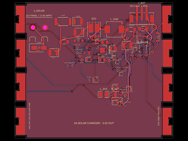 Similar packageShiboSoftwareDev/solar-battery-charger-moduleThis hardware setup integrates a solar panel, a lithium-ion battery, and a multi-rail buck converter with a battery charging IC, protection circuitry, and monitoring components, enabling solar power harvesting, battery charging, and power distribution in an embedded system.
 Discover something newimrishabh18/fitness_watchThis circuit integrates an ESP-12E microcontroller with various sensors and peripherals, including a AO3400A MOSFET for switching loads, to enable wireless control and sensor data processing.