pixalynx/pixal-gps
These files define two separate printed circuit boards: a small, two-layer battery cartridge with protection circuitry and contact pads for a pouch cell, and a larger, two-layer wireless charging dock featuring USB-C input, a resonant coil, and wireless power transmission components.
- Version
- 0.1.2
- License
- unset
- Stars
- 0
research/jlcpcb-stackup.md
# JLCPCB manufacturing facts for a 4-layer LTE-M + GNSS RF board

Research date: 2026-09-14. Every number below was read from the page whose URL is given next to it (WebFetch, or the JLCPCB
impedance calculator driven in the browser). Anything not found on a fetched page is marked **UNVERIFIED**.
Formula-derived numbers are labelled "computed" and the formula is stated.

---

## 1. JLCPCB 4-layer controlled-impedance stack-ups

Source: https://jlcpcb.com/impedance (current page; 18 four-layer options, thickness choices 0.8 / 1.0 / 1.2 / 1.6 / 2.0 mm,
outer copper 1 oz or 2 oz, inner 0.5 / 1 / 2 oz). All 4-layer entries on that page show outer copper 0.035 mm and inner copper 0.0152 mm.

### 1.1 Material constants (https://jlcpcb.com/impedance)

| Item | Value |
|---|---|
| Prepreg 7628 Dk | 4.4 |
| Prepreg 3313 Dk | 4.1 |
| Prepreg 2116 Dk | 4.16 |
| Prepreg 1080 Dk | 3.91 |
| Core Dk | 4.6 |
| Solder mask: coating above substrate C1 | 1.2 mil |
| Solder mask: coating above trace C2 | 0.6 mil |
| Solder mask: coating between traces C3 | 1.2 mil |
| Solder mask Dk (CEr) | 3.8 |

Note: the older JLCPCB page https://cart.jlcpcb.com/client/template/placeOrder/impedance.html still lists 7628 as Dk 4.6 and
3313 as Dk 4.05, and the older calculator template https://cart.jlcpcb.com/client/template/placeOrder/impedanceCalculation.html
uses "JLC7628: H1=7.10 mil, Er1=4.60, T1=1.40, C1=0.80, C2=0.50, CEr=3.80" and "JLC3313: H1=3.50 mil, Er1=4.05".
The current /impedance page and the live calculator (section 2) supersede those; the discrepancy is recorded so nobody
mixes the two parameter sets.

### 1.2 1.6 mm stack-ups (https://jlcpcb.com/impedance; finished-thickness labels from the calculator https://jlcpcb.com/pcb-impedance-calculator)

| Stack-up | L1 Cu | L1-L2 dielectric | L2 Cu | Core | L3 Cu | L3-L4 dielectric | L4 Cu | Calculator label |
|---|---|---|---|---|---|---|---|---|
| **JLC04161H-7628** | 0.035 | 7628 0.2104 mm ("7628, RC 49%, 8.6 mil" -> 8.28 mil after lamination) | 0.0152 | 1.065 mm ("1.1mm H/HOZ with copper", 41.93 mil) | 0.0152 | 7628 0.2104 | 0.035 | "Standard / Finished thickness 1.59mm +-10%" |
| **JLC04161H-3313** | 0.035 | 3313 0.0994 mm ("3313 RC57% 4.2mil" -> 3.91 mil) | 0.0152 | 1.265 mm ("1.3mm H/HOZ with copper", 49.80 mil) | 0.0152 | 3313 0.0994 | 0.035 | "Finished thickness 1.56mm +-10%" |
| **JLC04161H-2116** | 0.035 | 2116 0.1164 mm | 0.0152 | 1.265 mm | 0.0152 | 2116 0.1164 | 0.035 | "Special / Finished thickness 1.6mm +-10%" |
| JLC04161H-1080 | 0.035 | 1080 0.0764 mm | 0.0152 | 1.265 mm | 0.0152 | 1080 0.0764 | 0.035 | "Finished thickness 1.52mm +-10%" |
| JLC04161H-3313A | 0.035 | 3313 0.107 + 3313 0.0994 (0.2064 total) | 0.0152 | 1.065 mm | 0.0152 | same | 0.035 | "Special / 1.58mm" |
| JLC04161H-7628A | 0.035 | 7628 0.218 + 1080 0.0764 | 0.0152 | 0.865 mm | 0.0152 | same | 0.035 | "Special / 1.55mm" |
| JLC04161H-1080A | 0.035 | 1080 0.084 + 1080 0.0764 | 0.0152 | 1.065 mm | 0.0152 | same | 0.035 | "Special / 1.49mm" |
| JLC04161H-2116A | 0.035 | 2116 0.124 + 7628 0.218 + 2116 0.1164 | 0.0152 | 0.6 mm | 0.0152 | same | 0.035 | "Special / 1.62mm" |
| JLC04161H-2116B | 0.035 | 2116 0.124 + 7628 0.2104 | 0.0152 | 0.865 mm | 0.0152 | same | 0.035 | "Special / 1.63mm" |
| JLC04161H-2116C | 0.035 | 2116 0.124 + 1080 0.0764 | 0.0152 | 1.065 mm | 0.0152 | same | 0.035 | "Special / 1.57mm" |
| JLC04161H-2116D | 0.035 | 2116 0.124 + 7628 0.2104 | 0.0152 | 0.7 mm | 0.0152 | same | 0.035 | "Special / 1.47mm" |
| JLC04161H-2116E | 0.035 | 2116 0.124 + 2116 0.1164 | 0.0152 | 0.865 mm | 0.0152 | same | 0.035 | "1.45mm" |
| JLC04161H-7628B | 0.035 | 7628 0.218 + 7628 0.218 + 2116 0.1164 | 0.0152 | 0.4 mm | 0.0152 | same | 0.035 | "Special / 1.60mm" |
| JLC04161H-7628C | 0.035 | 7628 0.218 + 7628 0.218 + 7628 0.2104 | 0.0152 | 0.15 mm | 0.0152 | same | 0.035 | "Special / 1.54mm" |
| JLC04161H-7628E | 0.035 | 7628 0.218 + 7628 0.2104 | 0.0152 | 0.6 mm | 0.0152 | same | 0.035 | "1.56mm" |
| JLC04161H-7628F | 0.035 | 7628 0.218 + 7628 0.218 + 7628 0.2104 | 0.0152 | 0.25 mm | 0.0152 | same | 0.035 | "1.64mm" |
| JLC04161H-7628G | 0.035 | 7628 0.218 + 7628 0.218 + 1080 0.0764 | 0.0152 | 0.5 mm | 0.0152 | same | 0.035 | "1.63mm" |
| "No requirement" (default, no impedance control) | 0.035 | 7628 0.2104 | 0.0152 | 1.065 | 0.0152 | 7628 0.2104 | 0.035 | same geometry as JLC04161H-7628 |

Copper thickness legend used by JLCPCB: 1 oz outer = 1.38 mil = 0.035 mm; "H/HOZ" inner = 0.60 mil = 0.0152 mm (0.5 oz).
Only JLC04161H-7628 is tagged "Standard" in the calculator; the calculator states: "The first stack-up calculated below is
highly recommended as it has lowest cost and quickest turn-around." (https://jlcpcb.com/pcb-impedance-calculator)

### 1.3 Thinner 4-layer options (0.8 mm, 1.0 mm, 1.2 mm)

Source: https://cart.jlcpcb.com/client/template/placeOrder/impedance.html (older JLCPCB page, same copper: L1/L4 0.035 mm,
L2/L3 0.0152 mm). The current /impedance page has a thickness selector whose 0.8/1.0 mm entries were not captured by the
fetch, so treat these as "JLCPCB-published but from the older page" and confirm in the calculator by selecting PCB Thickness
0.8 / 1.0 before ordering.

| Stack-up | Total | L1-L2 prepreg | Core | L3-L4 prepreg |
|---|---|---|---|---|
| JLC04081H-7628 | 0.8 mm | 7628 0.2104 mm | 0.2 mm | 7628 0.2104 mm |
| JLC04081H-3313 | 0.8 mm | 3313 0.0994 mm | 0.45 mm | 3313 0.0994 mm |
| JLC04101H-7628 | 1.0 mm | 7628 0.2104 mm | 0.4 mm | 7628 0.2104 mm |
| JLC04101H-3313 | 1.0 mm | 3313 0.0994 mm | 0.7 mm | 3313 0.0994 mm |
| JLC04121H-7628 | 1.2 mm | 7628 0.2 mm | 0.7 mm | 7628 0.2 mm |
| JLC04121H-3313 | 1.2 mm | 3313 0.0994 mm | 0.865 mm | 3313 0.0994 mm |

Design consequence: the L1-to-L2 dielectric (0.2104 mm for 7628, 0.0994 mm for 3313) is the same at every board thickness,
so the 50 ohm RF trace geometry does not change if the board is thinned to 1.0 or 0.8 mm; only the core changes.
The page states: "The PCB will be strictly produced in accordance with the following stackup."

### 1.4 Impedance-control terms and surcharge

- Tolerance: "Impedance control ... 4/6/8/10/12/14/16/18/20/.../32 layers", "+-10%" standard, "+-5%" available upon request
  (https://jlcpcb.com/capabilities/pcb-capabilities).
- "For orders with 'Impedance Control' selected as 'Yes', our factory will control the impedance within a tolerance of +-10%."
  "If you choose 'No', we will not control the impedance, but we will ensure that the line width and spacing are within a
  tolerance of +/-20%." "Impedance control is not yet available for double-sided boards."
  (https://jlcpcb.com/blog/beginners-guide-to-impedance-control-in-pcb)
- "we offer standard free impedance testing (impedance tolerance +-20%) and precision impedance testing (chargeable)";
  "The PP thickness in the laminate structure is the thickness after lamination and is not the thickness as provided by the
  supplier" (https://jlcpcb.com/help/article/multi-layer-pcb-standard-laminated-structures).
- Track width tolerance "+-20%" (https://jlcpcb.com/capabilities/pcb-capabilities).
- Impedance-control surcharge in dollars: **not published on any fetched help/capability page**. The "In what cases will there be
  charged extra?" article (https://jlcpcb.com/help/article/in-what-cases-will-there-be-charged-extra) does not list impedance
  control at all. See section 7 for what the live quote page showed.
- Impedance control requires picking one of the named stack-ups when "Impedance Control = Yes" is chosen on the order form;
  the calculator's user guide says to "Use the JLCPCB Impedance Calculator in conjunction with your selected laminate structure
  to design the line width and spacing" (https://jlcpcb.com/help/article/multi-layer-pcb-standard-laminated-structures).
  Calculator geometry assumptions: "Trace top width" = "Trace base width - 0.7 mil"; base solder mask "1.2 mil", "0.6 mil" over
  copper; 4-8 layer material "Nan Ya Plastics NP-155F" core with 7628 / 3313(2313) / 1080 / 2116 prepregs; impedance ranges
  "20 to 90 ohm for single-ended and 50 to 150 ohm for differential"; structures: Coplanar Single Ended, Coplanar Differential
  Pair, Single Ended (Non coplanar), Differential Pair (Non coplanar) (https://jlcpcb.com/help/article/User-Guide-to-the-JLCPCB-Impedance-Calculator).
  The live calculator dropdown additionally offers "Coplanar Single Ended (without solder mask)".

---

## 2. 50 ohm trace widths, L1 referenced to L2

### 2.1 JLCPCB's own calculator (https://jlcpcb.com/pcb-impedance-calculator, run interactively 2026-09-14)

Settings: Board type Rigid, 4 layers, PCB thickness 1.6, inner copper 0.5 oz, outer copper 1 oz, unit mil, 50 ohm,
signal layer L1, bottom reference L2.

| Stack-up | Structure | Gap (trace to copper) | JLCPCB result | in mm |
|---|---|---|---|---|
| JLC04161H-7628 | Single Ended (Non coplanar) = microstrip | - | 14.1200 mil | **0.359 mm** |
| JLC04161H-3313 | Single Ended (Non coplanar) | - | 5.9400 mil | **0.151 mm** |
| JLC04161H-3313A | Single Ended (Non coplanar) | - | 13.5700 mil | 0.345 mm |
| JLC04161H-7628 | Coplanar Single Ended (CPWG) | 9.84 mil = 0.25 mm | 12.6100 mil | **0.320 mm** |
| JLC04161H-3313 | Coplanar Single Ended (CPWG) | 9.84 mil = 0.25 mm | 5.8800 mil | **0.149 mm** |
| JLC04161H-3313 | Coplanar Single Ended (CPWG) | 20 mil = 0.508 mm (calculator default) | 5.8800 mil | 0.149 mm |

Observations: on the 3313 stack-up the CPWG width is independent of the gap in JLCPCB's solver (0.25 mm and 0.51 mm gaps both
give 5.88 mil) because the 0.0994 mm dielectric dominates; on 7628 a 0.25 mm gap pulls the width from 0.359 to 0.320 mm.
Runs at 0.20 mm and 0.30 mm gaps were not captured from the calculator (the browser pane stopped accepting clicks); the
computed values below bracket them.

### 2.2 Computed cross-check (script: scratchpad/research/z0calc.py)

Microstrip: Hammerstad-Jensen closed form (Z01(u)=(eta0/2pi) ln(F(u)/u + sqrt(1+(2/u)^2)), F(u)=6+(2pi-6)exp(-(30.666/u)^0.7528),
eps_eff(u)=(er+1)/2+(er-1)/2 (1+10/u)^(-a b)) with the H&J finite-thickness correction, t = 0.035 mm, no solder mask.
CPWG: conductor-backed coplanar waveguide conformal-mapping formula (Wadell): k = W/(W+2G), k1 = tanh(pi W/4h)/tanh(pi(W+2G)/4h),
eps_eff = (1 + er K(k')/K(k) K(k1)/K(k1')) / (1 + K(k')/K(k) K(k1)/K(k1')), Z0 = 60pi/(sqrt(eps_eff) (K(k)/K(k') + K(k1)/K(k1'))),
zero-thickness copper, no mask. Inputs: h = L1-L2 prepreg thickness and Dk from section 1.1.

| Stack-up (h, Dk) | Microstrip W for 50 ohm | CPWG W, gap 0.20 mm | gap 0.25 mm | gap 0.30 mm |
|---|---|---|---|---|
| JLC04161H-7628 (0.2104 mm, 4.4) | 0.387 mm (0.374 mm if Dk 4.6) | 0.376 mm | 0.389 mm | 0.398 mm |
| JLC04161H-3313 (0.0994 mm, 4.1) | 0.186 mm (0.188 mm if Dk 4.05) | 0.206 mm | 0.210 mm | 0.213 mm |
| JLC04161H-2116 (0.1164 mm, 4.16) | 0.218 mm | 0.235 mm | 0.240 mm | 0.244 mm |
| JLC04161H-1080 (0.0764 mm, 3.91) | 0.146 mm | 0.168 mm | 0.171 mm | 0.173 mm |

Sanity values (microstrip, 7628): W 0.30 mm -> 57.5 ohm, 0.35 -> 52.9, 0.38 -> 50.5, 0.40 -> 49.0 ohm.
Sanity values (microstrip, 3313): W 0.15 mm -> ~52 ohm (interpolated), 0.20 -> 48.0, 0.25 -> 42.0 ohm.

Why JLCPCB's widths are narrower than the bare formula (0.359 vs 0.387 mm; 0.151 vs 0.186 mm): JLCPCB's solver includes the
solder mask (Dk 3.8, 1.2 mil / 0.6 mil) and the trapezoidal trace (top = base - 0.7 mil), both of which lower Z0 for a given width.
Use JLCPCB's numbers for the fab drawing; with "Impedance Control = Yes" the factory tunes the width to hit 50 ohm +-10%.

Design note (from the numbers above, not from JLCPCB): the JLC04161H-3313 50 ohm line is only 0.15 mm wide, so the +-20% width
tolerance (+-0.03 mm) and copper loss matter more; JLC04161H-7628 gives a 0.32-0.36 mm line, is the "Standard" (cheapest,
fastest) stack-up, and its 0.2104 mm L1-L2 spacing is identical on the 0.8 mm and 1.0 mm variants.

---

## 3. PCB fabrication capabilities relevant to a 4-layer RF board

Primary source: https://jlcpcb.com/capabilities/pcb-capabilities (fetched 2026-09-14). Extra-charge rules:
https://jlcpcb.com/help/article/in-what-cases-will-there-be-charged-extra.

| Item | JLCPCB value | Source |
|---|---|---|
| Min track/space, multilayer, 1 oz | "0.09 / 0.09 mm (3.5 / 3.5 mil)"; 3 mil accepted in BGA fan-outs; inner layers same as outer | pcb-capabilities |
| Min track/space, 2 oz (multilayer) | "0.15 / 0.15 mm (6 / 6 mil)" | pcb-capabilities |
| Track width tolerance | "+-20%" | pcb-capabilities |
| Surcharge for 3.0-3.5 mil trace/space on 4-8 layer boards | "20%" (difficulty process) | in-what-cases-will-there-be-charged-extra |
| Min via | "0.15 mm hole size / 0.25 mm via diameter" (multilayer; the page now shows the same for 2-layer) | pcb-capabilities |
| Min annular ring (PTH) | ">=0.20mm"; multilayer 1 oz: "Recommended 0.20 mm or above; absolute minimum 0.15 mm"; 2-layer: recommended 0.25, absolute min 0.18 | pcb-capabilities |
| Via hole-to-hole / via hole-to-track / pad hole-to-hole | 0.2 mm / 0.2 mm / 0.45 mm | pcb-capabilities |
| NPTH pad | ">=0.45mm" ring; min NPTH hole 0.50 mm | pcb-capabilities |
| Min plated slot (multilayer) | 0.35 mm; non-plated slot 1.0 mm | pcb-capabilities |
| PTH hole tolerance | "+0.13 / -0.08 mm" | pcb-capabilities |
| Board thickness tolerance (>=1.0 mm) | "+-10%" | pcb-capabilities |
| Outline tolerance | routed "+-0.2 mm (regular precision); +-0.1 mm (high precision)"; V-cut "+-0.4 mm" | pcb-capabilities |
| 4-layer thickness list | impedance page (controlled-impedance stack-ups): 0.8 / 1.0 / 1.2 / 1.6 / 2.0 mm. Live order form with 4 layers selected (2026-09-14): "PCB Thickness 0.4mm 0.6mm 0.8mm 1.0mm 1.2mm 1.6mm 2.0mm" | jlcpcb.com/impedance ; https://cart.jlcpcb.com/quote |
| Board size | min "3 x 3 mm"; max (FR4 4-layer) "663 x 593 mm" | pcb-capabilities |
| Copper weight, 4-layer | outer "1 oz / 2 oz"; inner "0.5 oz / 1 oz / 2 oz" | pcb-capabilities |
| Blind/buried vias | not supported (standard rigid service) | pcb-capabilities |
| Via covering options | Tented, Untented, Plugged, "Epoxy Filled & Capped", "Copper paste Filled&Capped"; plugged/epoxy-filled via hole "should not be larger than 0.5 mm"; untented vias need >=0.2 mm to other exposed copper unless ENIG | https://jlcpcb.com/help/article/pcb-via-covering |
| Via-in-pad (epoxy filled & capped / POFV) | "compatible with via diameters 0.15-0.55mm" (pcb-capabilities); "via-in-pad on 6-20 layer PCBs are upgraded to POFV ... for free" while "POFV for 4-layer PCBs still requires charges"; via hole size "0.2 to 0.5 mm", cap plating "up to 25um" | https://jlcpcb.com/news/free-via-in-pad-6-20-layer-pcbs-pofv ; "For 6-layer and above multi-layer boards, resin filling is now available for free" (pcb-via-covering) |
| Via-in-pad cost on 4-layer | dollar amount **UNVERIFIED** on help pages (only "still requires charges"); see section 7 | - |
| Solder mask bridge (sliver/dam) | "0.10mm" for 1 oz green/red/yellow/blue/purple; "0.13 mm" for black/white; "0.20 mm" for 2 oz; keep ">=0.09 mm clearance between soldermask openings and neighboring traces" | pcb-capabilities |
| Surface finishes | "HASL (leaded / lead-free), ENIG, OSP" (pcb-capabilities); ENIG gold "1 or 2 microinches", nickel "approximately 3-6 micrometers" (https://jlcpcb.com/help/article/jlcpcb-surface-finish) | |
| ENIG price | base ENIG price not on help pages (**UNVERIFIED**, see section 7); surcharge when ENIG area >30% of board: 1U" "$0.8992/m2 ... for every 1% for the portion exceeding 30%", 2U" "$1.7985/m2" | in-what-cases-will-there-be-charged-extra |
| ENIG 2u" free upgrade | search snippet says "For all 6-20 layer PCBs, JLCPCB is upgrading the immersion gold thickness to 2u" at no additional cost" (https://jlcpcb.com/news/free-upgrade-to-enig-2u) - page returned 404 when fetched, so **UNVERIFIED**; 4-layer boards therefore get 1u" unless 2u" is selected/charged | |
| Castellated holes | pcb-capabilities: "Min. Castellated Holes: 0.5mm", hole to board edge >=1 mm, hole spacing >=0.5 mm, min PCB 10 x 10 mm, min thickness 0.6 mm. Help article: "Hole size and space need to be 0.6 mm at least"; order form "Yes": "made with a special process and extra cost will be charged"; "No": "still be made but with the ordinary process, so the quality is not promised". Design blog: "Castellated hole diameter size >= 0.6 mm" (0.8-1.0 mm recommended), "Castellated hole edge to hole edge >= 0.6 mm", annular ring "0.25 mm (absolute limit 0.18 mm)", "Board edge to castellated pad (A) >= 1.0 mm", >=3.0 mm from board corners (5.0 mm recommended), pads extend >=0.5 mm inward, min board 10 x 10 mm, CNC-milled edges only (no V-cut), ENIG mandatory for edge-parallel slots >=5 mm long | pcb-capabilities ; https://jlcpcb.com/help/article/what-is-castellated-holes ; https://jlcpcb.com/blog/castellated-pcbs-introduction-and-design-requirements |
| Edge plating | min "10 x 10mm"; "copper-plated with ENIG treatment; HASL not supported"; at least 3 breaks for support tabs | pcb-capabilities |
| Small-hole surcharge | article lists extra cost cases for holes below the "diameter of >=0.3mm" standard - exact fee for 0.15-0.3 mm drills on 4-layer not stated (**UNVERIFIED**) | in-what-cases-will-there-be-charged-extra |
| Other listed extras | edge finishing "$0.02/pcs" (boards 1.5-3 cm) / "$0.05/pcs" (<1.5 cm); >150,000 drill holes/m2; boards >650 cm2; keyboard PCBs "$16.41+$49.25/m2"; expedited panel "$15.71 per design" | in-what-cases-will-there-be-charged-extra |

### 3.1 Order-form options as displayed on https://cart.jlcpcb.com/quote (read from the live page, 2026-09-14, 4 layers, 5 pcs)

- Base material: FR-4, Flex, Aluminum, Copper Core, Rogers, PTFE Teflon, HDI. Layers: 1, 2, 4, then "High Precision PCB" 6-16.
- PCB Thickness: 0.4 / 0.6 / 0.8 / 1.0 / 1.2 / 1.6 / 2.0 mm. Colours: Green, Purple, Red, Yellow, Blue, White, Black.
- Material Type: FR4 TG135, FR4 TG155, Nan Ya NP-140F, KB6164 - TG135, Nan Ya NP-155F, KB-6165 - TG155, S1141 TG140, S1000H TG155.
- Surface Finish: OSP, HASL(with lead), LeadFree HASL, ENIG (no hard-gold / ENEPIG / immersion-silver choice on the standard form).
- High-spec options: Outer Copper Weight 1 oz / 2 oz; Inner Copper Weight 0.5 oz / 1 oz / 2 oz; "Specify Stackup: No / Yes"
  with an "Impedance calculator >" link (this is where a JLC0416xH stack-up is chosen, i.e. impedance control requires
  "Specify Stackup = Yes"); Via Covering: Plugged, Untented, Epoxy Filled & Capped, Copper paste Filled & Capped, Tented;
  Via Plating Method: Not Specified, Conductive Adhesive, Horizontal Electroless Copper Plating;
  "Min via hole size/diameter": 0.3mm/(0.4/0.45mm), 0.25mm/(0.35/0.4mm), 0.2mm/(0.3/0.35mm), 0.15mm/(0.25/0.3mm), 0.1mm/(0.2/0.25mm)
  (first number = drill, bracketed pair = via pad diameter options - exact meaning of the pair see 3.2);
  Board Outline Tolerance +-0.2mm (Regular) / +-0.1mm (Precision); Electrical Test: Flying Probe Fully Test;
  Gold Fingers No/Yes; Castellated Holes No/Yes; Press-Fit Hole; Edge Plating No/Yes; Blind Slots; UL Marking; Backdrill; Humidity Indicator Card.
- Baseline "Charge Details" for a 4-layer, 5-pc order before touching any option: "Special Offer $7.00", "Via Covering $0.00",
  "Surface Finish $0.00", "PCB Build Time 3-4 days $0.00", "Calculated Price ... $7.00" (the form itemises each option's charge,
  which is how the surcharges in section 7 were read).

### 3.2 Meaning of the "Min via hole size/diameter" option pairs

The capabilities page states the multilayer minimum as "0.15 mm hole size / 0.25 mm via diameter"; the order form's
"0.15mm/(0.25/0.3mm)" therefore reads as drill 0.15 mm with a 0.25 mm (or 0.3 mm) via pad. Which copper weight or layer
each bracketed value applies to is not explained on any fetched page (the customer Q&A
https://jlcpcb.com/help/answers/detail/110-minimum%20via%20size%20vs.%20minimum%20annular%20ring%20size is unanswered) -
**UNVERIFIED**. For an RF board with 0.5 oz inner / 1 oz outer copper, a 0.2 mm drill / 0.4 mm pad via (or 0.25/0.45 mm)
stays inside every stated minimum (drill >=0.15 mm, ring >=0.2 mm recommended) without relying on the option semantics.

---

## 4. SMT assembly capabilities

Sources: https://jlcpcb.com/capabilities/pcb-assembly-capabilities (the detailed table; the URL
https://jlcpcb.com/capabilities/smt-assembly-capabilities is a marketing page that only says "Reliable assembly of ultra-small
components (01005, 0201)", "QFN, QFP, BGA, and LGA", "Single-Sided and Double-Sided Assembly", "Minimum pitch (>=0.35 mm)"),
https://jlcpcb.com/help/article/pcb-assembly-price, https://jlcpcb.com/help/article/pcb-assembly-faqs-part-2.

| Item | Economic PCBA | Standard PCBA |
|---|---|---|
| Assembly sides | single-sided placement | single and double-sided |
| Layer counts | 2/4/6-layer boards | 1-32 layers |
| PCB thickness | 0.8-1.6 mm | no limit |
| Single PCB size | 10 x 10 to 470 x 500 mm | 70 x 70 to 460 x 500 mm |
| Panel size | 10 x 10 to 250 x 250 mm | 70 x 70 to 250 x 250 mm |
| Order volume | 2-50 pcs | 2-80,000 pcs |
| Min passive package | 0402 | 0201 (01005 also supported per FAQ part 2, "step stencil" recommended) |
| Min IC lead pitch | 0.4 mm | 0.35 mm |
| Min BGA pitch (centre-to-centre) | 0.5 mm | 0.35 mm |
| Surface finish / colour | "Limited" | "No limit" |
| Inspection | AOI, visual, X-ray for BGA/hidden joints | same; X-ray is applied automatically when BGA/QFN/LGA are in the BOM |

Price components (https://jlcpcb.com/help/article/pcb-assembly-price, quoted values):
- Setup fee: Economic "$8.18"; Standard "$25.56/Single-side", "$51.12/Double-side".
- Stencil: Economic "$1.53"; Standard "$8.21/Single-side assembly", "$16.42/Double-side assembly".
- SMT assembly: "$0.0016/joint" (Economic 1-100,000 joints; Standard 1-50,000, then $0.0013, then $0.0012).
- Feeder loading (this is the "extended parts fee"): Economic "$3.07 Extend" per extended part, basic parts $0
  ("all parts in the basic category qualify for $0 Feeder Loading Fees in Economic PCBA"); Standard "$1.53 Basic/Extend" per part.
- Manual assembly "$0.0164/joint" (1-10,000). X-ray inspection "$1.64/pc" (1-10 pcs) down to "$0.082/pc" (3,001-99,999).
- Single-board surcharge "$0.48 minimum per board"; large PCBs (>650 cm2) "$57.46".
- Double-sided price rule: only Standard PCBA is double-sided; it doubles the setup ($25.56 -> $51.12) and stencil ($8.21 -> $16.42) fees.

Component rotation / polarity (https://jlcpcb.com/help/article/pcb-assembly-faqs-part-2):
"if you don't know how to change the file, please just place your order, our engineers will review and fix the rotation and
polarity of the components based on the silkscreen markings before assembly." Polarity is judged from the silk layer, so add a
silkscreen polarity mark ("a triangle to point to cathode" or "a band to the side of cathode"); pick-and-place rotation is in
degrees, positive = counter-clockwise (https://jlcpcb.com/help/article/pick-place-file-for-pcb-assembly).

nRF9151 (LGA SiP) at JLCPCB: it is in the parts catalogue and assemblable -
nRF9151-LACA-R7, JLCPCB part "C22397843", package "LGA-113(12.1x11.1)", category "RF Modules" (Extended sourcing),
"X-ray Inspection Required", MSL 3, ECCN 5A992C, "The purchased components are stored in your JLCPCB parts library for future
PCBA orders only, and cannot be shipped separately" (https://jlcpcb.com/partdetail/24009643-nRF9151_LACAR7/C22397843).
Other listings: NRF9151-LACA-R C42236596 (https://jlcpcb.com/partdetail/NordicSemicon-NRF9151_LACAR/C42236596),
nRF9151-LACAA0A C9900150298 "LGA-113_11.1x12.1mm" (https://jlcpcb.com/partdetail/JLCPCBAssembly-nRF9151LACAA0A/C9900150298).
JLCPCB publishes no special statement about "SiP modules"; LGA is simply in the supported package list and triggers X-ray.
LGA pads on the nRF9151 are on a 0.5-1.0 mm class pitch, well inside both service tiers (pitch itself: see Nordic PS, not
re-verified here - **UNVERIFIED**).

---

## 5. Hard gold vs ENIG (spring-contact / pogo pads)

- Gold fingers: "Only when ENIG is chosen, the fingers for your PCB will be with gold, if you choose HASL surface treatment, then
  it will be covered with tin." Boards/panels with gold fingers must be >=50 mm on each side; no chamfer on boards <5 x 5 cm;
  no copper in the bevel zone (https://jlcpcb.com/help/article/jlcpcb-gold-fingers). I.e. JLCPCB fingers are ENIG (soft
  immersion gold), not electroplated hard gold.
- No fetched JLCPCB page states that electroplated hard gold or "selective hard gold" is offered. The customer question "Do your
  PCB edge connector fingers have hard gold plating or just ENIG like the rest of the pcb?" (2023-05-06) is unanswered
  (https://jlcpcb.com/help/answers/detail/72-Hard%20gold%20plating%20for%20edge%20connectors); "Do you offer ENEPIG Finish?"
  (2025-02-10) is also unanswered (https://jlcpcb.com/help/answers/detail/663-ENEPIG-Finish). -> Hard gold / selective hard
  gold / ENEPIG at JLCPCB: **UNVERIFIED / not offered on the standard order form as far as the fetched pages show**.
- ENIG spec: gold "1 or 2 microinches", nickel "approximately 3-6 micrometers"; OSP "cannot be used on wear-resistant,
  conductive contact surfaces such as mating gold fingers" (https://jlcpcb.com/help/article/jlcpcb-surface-finish).
- JLCPCB's blog (general industry text, not a JLCPCB offer): hard gold "thickness can reach 3-50u"", nickel "3 to 6 microns",
  IPC range "2 to 50 microinches" (https://jlcpcb.com/blog/pcb-gold-fingers). JLCPCB says nothing specific about pogo-pin test
  pads; the practical choice on their form is ENIG for low-cycle pogo/test pads - the live order form exposes a
  "Gold Thickness 1 U" / 2 U"" selector once ENIG is chosen (https://cart.jlcpcb.com/quote, observed 2026-09-14), so 2 U"
  ENIG is orderable on a 4-layer board at some surcharge (amount UNVERIFIED, section 7).
- JLCPCB carries pogo-pin parts in its assembly library (https://jlcpcb.com/parts/2nd/Connectors/Pogo_Pin_Spring_Probe_Connector_103).

---

## 6. RF bands the antenna must cover

### 6.1 LTE FDD bands (3GPP numbering; table values from https://en.wikipedia.org/wiki/LTE_frequency_bands, which mirrors 3GPP TS 36.101 Table 5.5-1)

| Band | Uplink (MHz) | Downlink (MHz) | Duplex spacing (MHz) | Common name |
|---|---|---|---|---|
| 1 | 1920-1980 | 2110-2170 | 190 | IMT |
| 2 | 1850-1910 | 1930-1990 | 80 | PCS |
| 3 | 1710-1785 | 1805-1880 | 95 | DCS |
| 4 | 1710-1755 | 2110-2155 | 400 | AWS-1 |
| 5 | 824-849 | 869-894 | 45 | Cellular (850) |
| 8 | 880-915 | 925-960 | 45 | Extended GSM (900) |
| 12 | 699-716 | 729-746 | 30 | Lower SMH (700) |
| 13 | 777-787 | 746-756 | -31 | Upper SMH (700) |
| 17 | 704-716 | 734-746 | 30 | Lower SMH (700) |
| 18 | 815-830 | 860-875 | 45 | Lower 800 (Japan) |
| 19 | 830-845 | 875-890 | 45 | Upper 800 (Japan) |
| 20 | 832-862 | 791-821 | -41 | Digital Dividend (EU 800) |
| 25 | 1850-1915 | 1930-1995 | 80 | Extended PCS |
| 26 | 814-849 | 859-894 | 45 | Extended Cellular |
| 28 | 703-748 | 758-803 | 55 | APT 700 |
| 66 | 1710-1780 | 2110-2200 | 400 | Extended AWS |

Union for the antenna: **699-960 MHz** (low band: B12/B17/B28/B13/B20/B26/B18/B5/B19/B8) and **1710-2200 MHz**
(high band: B3/B4/B66/B2/B25/B1). Nothing in 960-1710 MHz except GNSS.

### 6.2 nRF9151 band support (Nordic)

- "Cat-M1 - B1, B2, B3, B4, B5, B8, B12, B13, B18, B19, B20, B25, B26, B28, B66, B85, B106";
  "Cat-NB1/NB2 - B1, B2, B3, B4, B5, B8, B12, B13, B17, B19, B20, B25, B26, B28, B65, B66, B85. B106";
  "Single 50 ohm antenna interface"; "LGA package 12.1x11.1x1.2 mm"; "GPS L1 C/A supported", "QZSS L1 C/A supported"
  (https://docs.nordicsemi.com/r/bundle/ps_nrf9151/page/nrf9151_html5_keyfeatures.html).
- "Supports LTE bands from 700 MHz to 2.2 GHz through a single 50 ohm antenna pin"
  (https://docs.nordicsemi.com/r/bundle/ps_nrf9151/page/ip/radio_lte/doc/frontpage.html). Cat-M1 TX: frequency range
  698-1980 MHz, output impedance 50 ohm, Power Class 3 max 23 dBm, Power Class 5 max 20 dBm
  (https://docs.nordicsemi.com/r/bundle/ps_nrf9151/page/_tmp/alta.nrf9151/autodita/application.radiolte/parameters.rf_spec_tx_m1.html).
- Product page: "Certified Bands: 1-5, 8, 12, 13, 17-20, 25, 26, 28, 65, 66, 85", "700-2200 MHz (LTE)", "11x12x1 mm LGA"
  (https://www.nordicsemi.com/Products/nRF9151).
- GNSS input: "GPS receiver operation is time multiplexed with the LTE modem, and GPS and QZSS position can be received while
  the LTE modem is in RRC Idle mode, power saving mode (PSM), or completely deactivated." "External low-noise amplifier (LNA)
  with SAW filter recommended on the GPS antenna input." "GPS antenna pin is DC grounded." "There must be minimum 27dB
  attenuation to out of band power to avoid blocking high power RF signals to GPS receiver input."
  (https://docs.nordicsemi.com/r/bundle/ps_nrf9151/page/gps.html). So the SiP has a separate GPS antenna pin in addition to
  the LTE ANT pin (exact pin names not re-verified here - **UNVERIFIED**).

### 6.3 GNSS L1-band frequencies

| Signal | Centre frequency | Source |
|---|---|---|
| GPS L1 (C/A, P(Y), M, L1C) | 1575.42 MHz; C/A chip rate 1.023 Mcps (main lobe +-1.023 MHz) | https://gssc.esa.int/navipedia/index.php/GPS_Signal_Plan |
| Galileo E1 | 1575.420 MHz; receiver reference bandwidth 24.552 MHz | https://gssc.esa.int/navipedia/index.php/Galileo_Signal_Plan |
| BeiDou B1C / B1I | 1575.42 MHz / 1561.098 MHz | https://gssc.esa.int/navipedia/index.php/BeiDou_Signal_Plan |
| GLONASS L1 FDMA | f = 1602 MHz + k x 0.5625 MHz, k = -7..+6 (centres 1598.0625-1605.375 MHz); CDMA L1OC 1600.995 MHz | https://gssc.esa.int/navipedia/index.php/GLONASS_Signal_Plan |
| Upper L-band allocation | 1559-1610 MHz | https://gssc.esa.int/navipedia/index.php/GNSS_signal |

The nRF9151 only uses GPS/QZSS L1 C/A, so the GNSS antenna/filter requirement is 1575.42 MHz +-~2 MHz (a SAW centred at
1575.42 MHz with >=27 dB out-of-band rejection per Nordic); a wider 1559-1610 MHz passive antenna also covers Galileo/BeiDou B1C.

---

## 7. Live quote-page surcharges (order form https://cart.jlcpcb.com/quote)

Read from the itemised "Charge Details" panel on 2026-09-14 for: Standard PCB, FR-4, 4 layers, 50 x 50 mm, 5 pcs, all other
options at their defaults (1.6 mm, 1 oz outer / 0.5 oz inner, HASL, tented vias). These are quote-time values for this exact
configuration; they scale with area and quantity, so re-quote before ordering.

| Option toggled | Itemised charge shown | Running total | Notes |
|---|---|---|---|
| Baseline, nothing toggled | "Special Offer $7.00" | $7.00 | the promotional 4-layer price for 5 pcs |
| Via Covering = "Epoxy Filled & Capped" (via-in-pad / POFV) | "Via Covering $16.73" plus an automatically added line "Via Plating Method $3.31" | $27.04 | about $20 extra on this order; free only on 6+ layers (section 3) |
| Surface Finish = ENIG | "Surface Finish $16.80" | $43.84 | a "Gold Thickness 1 U" / 2 U"" selector appears; $16.80 is with the default 1 U"; 2 U" delta: see below |
| Edge Plating = Yes | "Edge Plating $50.28" | $94.12 | most expensive option by far; ENIG-only process |
| Specify Stackup = Yes (named JLC0416xH stack-up / impedance control) | see below | | |
| Castellated Holes = Yes | see below | | help page: "extra cost will be charged" |
| Gold Fingers = Yes | see below | | fingers are ENIG, not hard gold (section 5) |
| Min via 0.15mm/(0.25/0.3mm) | see below | | |

Not captured (the browser tab was navigated away by the environment three times while the toggle script ran; the four
rows below therefore stay **UNVERIFIED** and should be read off the quote page by hand - each option's charge appears as its
own line under "Charge Details" within a few seconds of clicking it):

- Specify Stackup = Yes / impedance control: no dollar figure captured. JLCPCB's published position is: impedance testing at
  +-20% is free and "precision impedance testing (chargeable)" (section 1.4); the calculator flags JLC04161H-7628 as the
  stack-up with "lowest cost and quickest turn-around", so expect any surcharge to apply to the non-"Standard" stack-ups
  (3313, 2116, 1080, and all "Special" variants) rather than to 7628.
- Castellated Holes = Yes: no figure captured; the help page only says "extra cost will be charged".
- Gold Fingers = Yes: no figure captured; per section 5 this yields ENIG-plated fingers, not hard gold.
- Min via 0.15mm/(0.25/0.3mm): no figure captured; the extra-charges article implies drills below 0.3 mm can carry a fee.
- ENIG 2 U": after selecting ENIG the form shows "Gold Thickness 1 U" 2 U""; the $16.80 above is at the 1 U" default and the
  2 U" increment was not captured.

---

## 8. Not verified / open items

- Impedance-control fee, 4-layer via-in-pad (POFV) fee, ENIG base fee, castellated-hole fee: no fixed number on JLCPCB help
  pages; only obtainable from the live quote (section 7).
- 0.8 / 1.0 mm stack-up numbers come from the older cart page; re-check in the calculator with the thickness selector.
- Hard gold / selective hard gold / ENEPIG: no JLCPCB page says they are offered; two customer questions are unanswered.
- ENIG 2u" free-upgrade news page returned 404 (snippet only).
- Capability-page 4-layer thickness list extracted inconsistently (0.4-2.0 vs 0.8-1.6); impedance page says 0.8/1.0/1.2/1.6/2.0.
Related Packages
 More from this authorpixalynx/esp32-gps-cellular-trackerThis code defines a hardware layout comprising a Wi-Fi-enabled ESP32 module, GPS module, cellular GSM module, battery management components (including charger, protection circuits, and voltage regulators), USB-C connector, SIM card holder, RF components, and supporting passive components for a comprehensive GPS+Cellular tracker device.
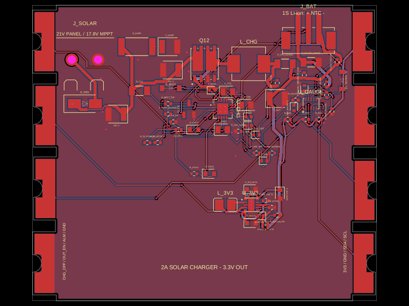 Similar packageShiboSoftwareDev/solar-battery-charger-moduleThis hardware setup integrates a solar panel, a lithium-ion battery, and a multi-rail buck converter with a battery charging IC, protection circuitry, and monitoring components, enabling solar power harvesting, battery charging, and power distribution in an embedded system.
 Discover something newimrishabh18/fitness_watchThis circuit integrates an ESP-12E microcontroller with various sensors and peripherals, including a AO3400A MOSFET for switching loads, to enable wireless control and sensor data processing.