pixalynx/pixal-gps
These files define two separate printed circuit boards: a small, two-layer battery cartridge with protection circuitry and contact pads for a pouch cell, and a larger, two-layer wireless charging dock featuring USB-C input, a resonant coil, and wireless power transmission components.
- Version
- 0.1.2
- License
- unset
- Stars
- 0
parts/Bq51013b.tsx
import type { ChipProps } from "tscircuit"
import { pad, via, outline, courtyard } from "../lib/footprints"

/** TI BQ51013B Qi (WPC v1.2 BPP) wireless-power receiver, VQFN-20 RHL 3.5 x 4.5 mm.
 * Pin numbers from the datasheet SLUSB62D pin table; land pattern from TI drawing
 * RHL0020A (docs/sources.md [bq51013b]): 20 lands 0.24 x 0.6 mm on a 0.5 mm pitch,
 * centre spans 3.3 mm (X) and 4.3 mm (Y), exposed pad 2.05 x 3.05 mm. The lands here
 * are 0.28 x 0.70 mm (JLC/EasyEDA C55663 uses 0.28 x 0.85) so the toe is inspectable.
 * Orientation: TI top view, long (4.5 mm) sides vertical. Pin 1 top-left on the short
 * side, numbering counter-clockwise: 1, 20 on top; 2-9 down the left; 10, 11 on the
 * bottom; 12-19 up the right. */
const Rhl20 = () => (
  <footprint>
    {pad(1, -0.25, 2.2, 0.28, 0.7)}
    {pad(20, 0.25, 2.2, 0.28, 0.7)}
    {[2, 3, 4, 5, 6, 7, 8, 9].map((p, i) => pad(p, -1.7, 1.75 - i * 0.5, 0.7, 0.28))}
    {pad(10, -0.25, -2.2, 0.28, 0.7)}
    {pad(11, 0.25, -2.2, 0.28, 0.7)}
    {[12, 13, 14, 15, 16, 17, 18, 19].map((p, i) => pad(p, 1.7, -1.75 + i * 0.5, 0.7, 0.28))}
    {pad(21, 0, 0, 2.05, 3.05)}
    {[[-0.5, -1.0], [0.5, -1.0], [-0.5, 0], [0.5, 0], [-0.5, 1.0], [0.5, 1.0]].map(([x, y]) => via(21, x, y, 0.25, 0.5))}
    {outline(3.5, 4.5)}
    <silkscreencircle pcbX={-1.05} pcbY={2.65} radius={0.15} strokeWidth={0.1} />
    {courtyard(4.3, 5.2)}
  </footprint>
)

export const bq51013bPins = {
  pin1: ["PGND2"], pin2: ["AC1"], pin3: ["BOOT1"], pin4: ["OUT"], pin5: ["CLAMP1"], pin6: ["COMM1"], pin7: ["CHG"],
  pin8: ["AD_EN"], pin9: ["AD"], pin10: ["EN1"], pin11: ["EN2"], pin12: ["ILIM"], pin13: ["TS_CTRL"], pin14: ["FOD"],
  pin15: ["COMM2"], pin16: ["CLAMP2"], pin17: ["BOOT2"], pin18: ["RECT"], pin19: ["AC2"], pin20: ["PGND1"], pin21: ["PGND", "EP"],
} as const

export const Bq51013b = (props: ChipProps<typeof bq51013bPins>) => (
  <chip
    {...props}
    manufacturerPartNumber="BQ51013BRHLR"
    supplierPartNumbers={{ jlcpcb: ["C55663"] }}
    pinLabels={bq51013bPins}
    internallyConnectedPins={[["PGND1", "PGND2", "PGND"]]}
    footprint={<Rhl20 />}
    cadModel={{ objUrl: "https://modelcdn.tscircuit.com/easyeda_models/assets/C55663.obj?uuid=d37a54d40c264d5d8e19accad3495803", rotationOffset: { x: 0, y: 0, z: 0 }, positionOffset: { x: 0, y: 0, z: 0 } }}
    schWidth={3.5}
    schHeight={6}
    schPinArrangement={{
      leftSide: { direction: "top-to-bottom", pins: ["AC1", "BOOT1", "COMM1", "CLAMP1", "AC2", "BOOT2", "COMM2", "CLAMP2", "AD", "AD_EN"] },
      rightSide: { direction: "top-to-bottom", pins: ["RECT", "OUT", "CHG", "EN1", "EN2", "ILIM", "FOD", "TS_CTRL"] },
      bottomSide: { direction: "left-to-right", pins: ["PGND1", "PGND2", "PGND"] },
    }}
    pinAttributes={{ OUT: { providesPower: true }, PGND: { requiresGround: true }, PGND1: { requiresGround: true }, PGND2: { requiresGround: true }, ILIM: { mustBeConnected: true }, TS_CTRL: { mustBeConnected: true }, AD: { mustBeConnected: true } }}
  />
)
Related Packages
 More from this authorpixalynx/esp32-gps-cellular-trackerThis code defines a hardware layout comprising a Wi-Fi-enabled ESP32 module, GPS module, cellular GSM module, battery management components (including charger, protection circuits, and voltage regulators), USB-C connector, SIM card holder, RF components, and supporting passive components for a comprehensive GPS+Cellular tracker device.
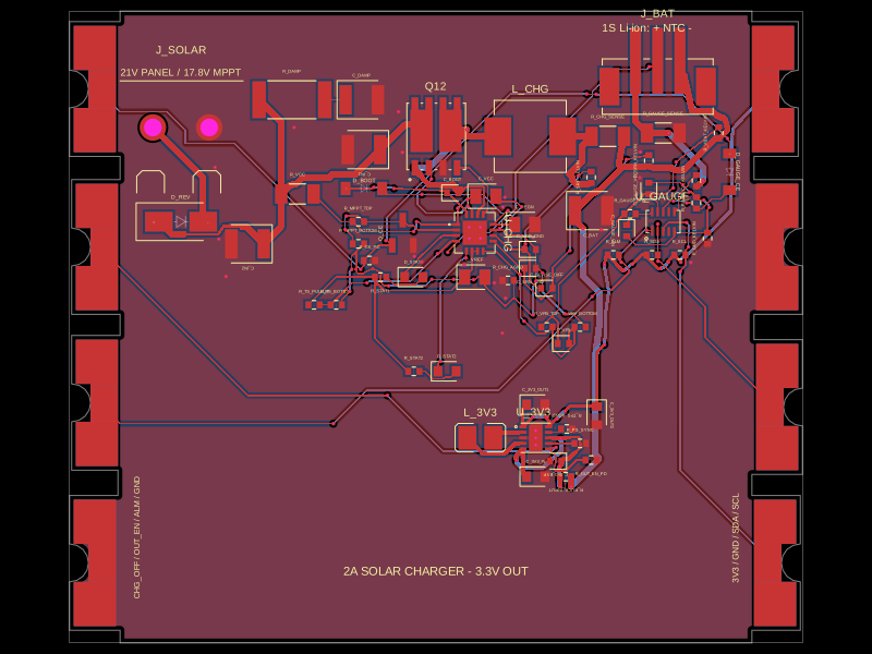 Similar packageShiboSoftwareDev/solar-battery-charger-moduleThis hardware setup integrates a solar panel, a lithium-ion battery, and a multi-rail buck converter with a battery charging IC, protection circuitry, and monitoring components, enabling solar power harvesting, battery charging, and power distribution in an embedded system.
 Discover something newimrishabh18/fitness_watchThis circuit integrates an ESP-12E microcontroller with various sensors and peripherals, including a AO3400A MOSFET for switching loads, to enable wireless control and sensor data processing.