pixalynx/pixal-gps
These files define two separate printed circuit boards: a small, two-layer battery cartridge with protection circuitry and contact pads for a pouch cell, and a larger, two-layer wireless charging dock featuring USB-C input, a resonant coil, and wireless power transmission components.
- Version
- 0.1.2
- License
- unset
- Stars
- 0
docs/routing.md
# Tracker routing flow (board A)

The tracker is 34 × 24 mm, four layers, with 395 lands and 65 nets on both sides. tscircuit's built-in capacity
autorouter did not converge on it: three full runs (default, 100× effort, and a phased variant; with and without
the ground mesh) all stalled at 46 % of the port-pathing phase after more than 30 minutes each, and a subcircuit
partition moved the placement. The copper is therefore produced in three explicit stages and every stage is
committed as source, so `bunx tsci build tracker.circuit.tsx` reproduces the routed board in about 20 s without
invoking any autorouter. Nothing on the board is autorouted at build time (`routingDisabled`); the native router can
be re-enabled for experiments with `PIXAL_AUTOROUTE=1`.

## 1. Hand-routed copper (source)

The LTE chain (ANT → π-match → J1), the GNSS chain (J2 → SAW → LNA → GPS) and the AUX/combined-antenna option are
explicit 0.32 mm coplanar legs in `tracker.circuit.tsx` (`rf_*` traces, board-frame points converted with
`lib/geometry.ts`; see `docs/rf.md`). A handful of non-RF legs are also hand-routed because no automatic pass could
place them: the LNA enable/supply crossing under the AUX line (`lna_ven`, `lna_vcc`), the LNA GND2/GND3 ties into its
paddle, the bias-T inductor stub (`rf_bias_stub`), the PMIC LSIN1–VOUT2 link under its top row, VBUSOUT to its
capacitor, and the Qi FOD node. Each carries a comment explaining the constraint.

## 2. Generated ground mesh (`routing/tracker-gnd.json`)

Every ground land is declared in the source (`GND_LANDS`; internally-bonded pin groups do not propagate net
membership to their other pins, so all 100 lands are listed). `scripts/gen-gnd-mesh.py` reads the unrouted build and
gives each land its own 0.4/0.2 mm via into the L2 plane 0.45 mm beyond the land (six candidate directions, 0.18 mm
clearance to every land, hole, board edge, earlier via and RF copper, 0.55 mm from the outline, and never inside the
0.6 mm escape lane in front of another part's chip lands). Lands with no free via spot are linked straight to a
stubbed neighbour on the same layer; the rest are listed as `unresolved` and left to stage 3, which connects them to a
neighbouring ground land on the surface (Freerouting never drops vias into the plane on its own).

## 3. Freerouting pass for signals and power (`routing/tracker-routes.json`)

```bash
./scripts/prepare-tracker-routing.sh          # empty JSONs -> placement build -> mesh -> build -> tmp/router/tracker.dsn
bun run route:run                             # Freerouting 1.9.0, 120 passes, 3-17 min -> tmp/router/tracker.ses
bun run route:import                          # -> routing/tracker-routes.json (+ tmp/router/tracker-import-report.json)
python3 scripts/widen-power-legs.py tracker   # power legs 0.20 -> 0.30 mm where the clearance audit allows; rebuilds
bun run check                                 # design assertions incl. land coverage, leg placement hash, DRC = 0
python3 scripts/check-clearance.py dist/tracker/circuit.json   # independent 0.10 mm copper / 0.30 mm edge audit
```

The DSN exporter writes every land as its own single-pin component (no footprint-frame assumptions), all existing
copper (RF legs, ground stubs, hand legs and their vias) as fixed wiring, the L2 ground plane as a power layer, 0.4 mm
edge keepouts and 1.0 mm keepouts around the SIM-socket peg holes on the three routing layers, a wire keepout corridor
(0.5 mm half-width) around every 50 Ω line on L1 and a via keepout under it on all layers so the reference plane stays
solid. Rules: 0.15 mm signal traces, 0.20 mm for the power rails during routing (VSYS, VBAT, VBUS_QI, VDD_NRF, RECT,
VBUSOUT, AC1/AC2, COIL1; widened to 0.30 mm afterwards), 0.25 mm ground, 0.12 mm clearance, 0.4/0.2 mm vias. Routing
power at 0.30 mm directly left every 0.30 mm QFN land unrouted, silently.

The importer parses the session file, verifies that every land came back exactly where it was exported, drops any
echoed fixed copper, and stitches the router's loose fragments per net into a graph (T-junctions split, vias join
layers, the L2 plane is a node). It then decomposes each net into land-to-land legs (shortest graph path from every
land to the nearest already-served land) and writes them in board coordinates together with the owning component's
centre and rotation. `lib/routed-traces.tsx` renders them as ordinary named `<trace pcbPath>` legs (the same mechanism
as the RF and ground copper), so the final board is plain source. Trunk copper shared by several legs of one net is
repeated in each leg (same-net overlap, electrically identical, DRC clean).

The JSON records the SHA-256 of the build it was routed against; `scripts/validate.ts` fails when a component named
by a leg has moved or rotated since, when any land on a multi-land net has no copper, or when core reports any PCB
error, so a placement change forces a re-route instead of silently rendering stale copper.

## What the router would not do, and the placement answers

Six passes were needed. Every land Freerouting left unrouted turned out to be a placement fault, not a router limit:

- a neighbouring capacitor's ground stub via parked in the escape lane of a chip land (U5.FOD, U3.SCL) → the mesh
  generator now keeps 0.6 mm escape lanes clear;
- two-pin capacitors facing the PMIC or the Qi receiver with their ground pin, so the signal pin sat behind it
  (C21 VSYS, C24 PVDD, C33 AC2, C30 BOOT1) → rotated so the connecting pin faces the chip;
- channels between chip lands and the nearest pads narrower than 0.64 mm (via 0.4 mm + 2 × 0.12 mm), where no via
  can escape (PMIC left column vs C21, PMIC top row vs the pogo pads, Qi receiver vs its resonant caps) → parts moved
  0.3–0.7 mm, the PMIC moved 0.5 mm down, the pull-up resistors re-spaced, the VANT capacitor moved to the top side;
- two nets needing vias in the same 0.25 mm window (LNA VEN/VCC under the AUX line) → hand-routed as fixed legs.

## Results

The board is fully routed: 234 traces, 186 vias, 0 placement errors, 0 DRC errors, 0 clearance findings below
0.10 mm (checked independently by `scripts/check-clearance.py`, which catches some 0.05-0.09 mm near-misses core's
own checker does not flag for hand-authored copper). All 342 design assertions across the three boards pass
(`bun run check`).

Five connections that six full Freerouting passes never completed, even with every other net already placed as
fixed copper, needed a purpose-built grid-search router instead (`scripts/hand-route-net.py`, BFS on a 0.1 mm grid
per layer, with a clear-via-spot search reused from the ground-mesh generator): `U1.P0_31`-`U6.INT1` (ACC_INT1),
`U3.VBUS`-`C22.pin1` (VBUS_QI), `U6.SCL`-`U1.P0_29` (I2C_SCL), `R13.pin1`-`R14.pin2` (QI_FOD), and a plane stub for
`C41.pin2` (GND); they are named `hand_*` in the source. Two of the five (ACC_INT1 and I2C_SCL) turned out to share
the same square millimetre of inner2 immediately south of the SiP, since P0_31 and P0_29 are adjacent pins escaping
in the same direction: a via placed directly next to the U6 accelerometer's target pad is provably unreachable from
there (confirmed by a whole-board flood fill), so both routes take the same kind of wide detour Freerouting itself
took for other nets in this area, and were generated one after the other so each treats the other's copper as a
fixed obstacle.
Related Packages
 More from this authorpixalynx/esp32-gps-cellular-trackerThis code defines a hardware layout comprising a Wi-Fi-enabled ESP32 module, GPS module, cellular GSM module, battery management components (including charger, protection circuits, and voltage regulators), USB-C connector, SIM card holder, RF components, and supporting passive components for a comprehensive GPS+Cellular tracker device.
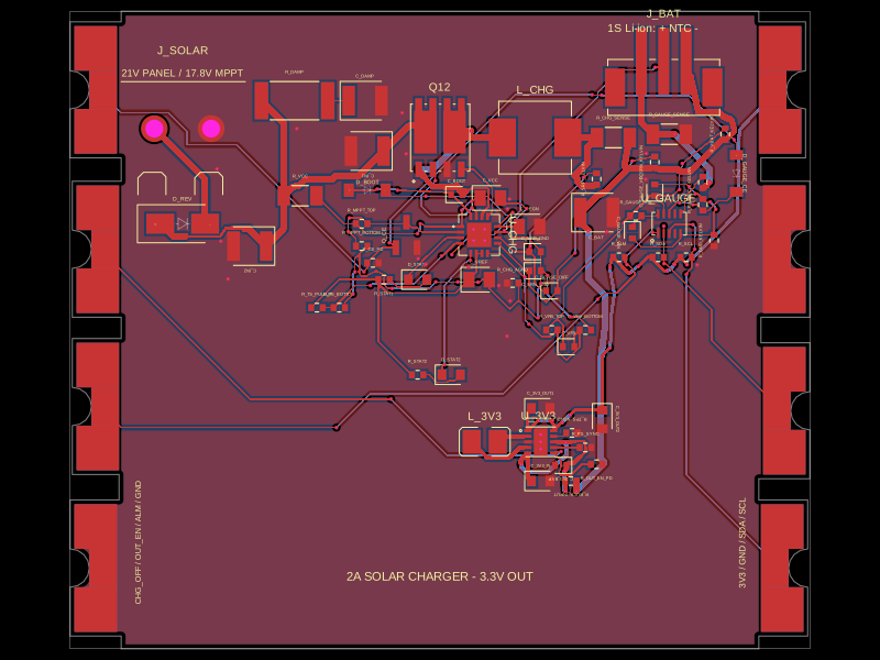 Similar packageShiboSoftwareDev/solar-battery-charger-moduleThis hardware setup integrates a solar panel, a lithium-ion battery, and a multi-rail buck converter with a battery charging IC, protection circuitry, and monitoring components, enabling solar power harvesting, battery charging, and power distribution in an embedded system.
 Discover something newimrishabh18/fitness_watchThis circuit integrates an ESP-12E microcontroller with various sensors and peripherals, including a AO3400A MOSFET for switching loads, to enable wireless control and sensor data processing.