pixalynx/pixal-gps
These files define two separate printed circuit boards: a small, two-layer battery cartridge with protection circuitry and contact pads for a pouch cell, and a larger, two-layer wireless charging dock featuring USB-C input, a resonant coil, and wireless power transmission components.
- Version
- 0.1.2
- License
- unset
- Stars
- 0
docs/power.md
# Power architecture, sleep current and battery selection

Sources: nPM1300 Product Specification v1.3, nPM1300 Hardware Design Guidelines (nwp_050), nPM1300 EK / reference layout v1.2 schematics, nRF9151 PS/HDG, Thingy:91 X schematic; cell datasheets as cited. See [sources.md](sources.md).

## Rails

```
Cartridge BAT+ ─ P1 ─┬─ C20 2.2 µF ─ nPM1300 VBAT
Qi receiver OUT (5 V) ─ C42/C43 ─ nPM1300 VBUS  (CC1/CC2 to GND: not a USB-C source)
nPM1300 VSYS ─ C21/C24/C25 3×10 µF ─┬─ FB1 22 Ω/6 A ─ C1,C2 1 µF ─ nRF9151 VDD (pin 14)      [3.0–5.5 V input]
                                     ├─ C3 47 µF, C4 10 µF (bulk, before the bead)
                                     ├─ LED anodes (D1 charging, D2 host) → LED1/LED2 5 mA sinks
                                     ├─ VOUT2 (BUCK2 disabled by VSET2 = GND, output tied to VSYS as in Nordic config 3)
                                     └─ LSIN1 → load switch 1 → VANT (active GNSS antenna bias, off by default)
nPM1300 BUCK1 (VSET1 47 k → 1.8 V, L1 2.2 µH, C26 10 µF) ─ V1V8 ─┬─ nRF9151 VDD_GPIO (C5 100 nF, C6 4.7 µF)
                                                                  ├─ nPM1300 VDDIO (C27 100 nF), I2C pull-ups
                                                                  ├─ LIS2DW12 VDD/VDD_IO/CS (C44 100 nF, C45 10 µF)
                                                                  └─ FB2 → SKY65943-11 VCC (LNA), CHG pull-up
nRF9151 SIM_1V8 (internal LDO) ─ C9 100 nF ─ TPD3F303 VCC clamp ─ SIM VCC (C46 10 nF at the socket)
nRF9151 DEC0 ─ C7 4.7 µF (exactly; Nordic: 10 µF "may be on the limit", 47 µF fails to boot)
```

Why this shape:

- The nRF9151 wants 3.0–5.5 V (3.2 V recommended minimum including ripple) on VDD and up to ~500 mA peaks; Nordic's Thingy:91 X feeds it from nPM1300 VSYS and its DK from a 5 V rail, and the HDG's input filter is C1–C4 + FB1 with "keep supply network impedance at the VDD pin below 0.2 Ω from 10 kHz to 50 kHz". Feeding VDD from VSYS (not from the battery contact) keeps the PMIC's ship mode able to cut the whole system.
- VDD_GPIO is an input (1.7–3.6 V). Both Nordic boards use nPM1300 VOUT1 = 1.8 V (VSET1 47 kΩ). Sequencing rules ("apply VDD and ENABLE before VDD_GPIO", "VDD_GPIO at least 6 ms after ENABLE and VDD") are met the way Nordic meets them: VSYS is present before the buck finishes its 1.2 ms start-up? — no: BUCK1 starts as soon as VSYS is valid, so the 6 ms margin is *not* guaranteed by hardware. Nordic's own Thingy:91 X wires it identically, and ENABLE is tied to VDD through R1 (10 kΩ) as the HDG allows. If bring-up shows leakage or undefined GPIO state at power-up, the fix is a GPIO-controlled BUCK1 enable (BUCKENCTRL) driven 6 ms after VSYS — no PCB change.
- BUCK2 and LDO2 are unused and terminated exactly as Nordic's reference "config 3" (VSET2 → GND, VOUT2 → VSYS, SW2 open, PVSS2 → GND, LSIN2/LSOUT2 → GND). LDO1 is used as a 100 mA load switch for the optional active-antenna bias. Its 1 µF output capacitor (C29) sits on the top side next to the bias-T inductor L3 rather than at the LSOUT1 land: the PMIC's top row of lands faces the battery pogo pads and has no room for the capacitor's ground via. That is fine for load-switch use; if firmware ever configures LDO1 as a regulator, Nordic's stability guidance wants the capacitor back at the pin (Rev B item).
- The nPM1300's VBUS input limit powers up at 100 mA (factory OTP, not changeable) and only rises when the host writes `VBUSINILIM0` and `TASKUPDATEILIMSW`; it reverts on every re-dock. CC1/CC2 are grounded ("If USB Type-C configuration is not used, CC1 and CC2 can be left floating or connected to ground").
- Charger settings are registers, no resistors: ICHG 32–800 mA in 2 mA steps, VTERM 4.00–4.45 V (default 3.60 V until configured), NTC 10 kΩ β3380 selected by `ADCNTCRSEL`, JEITA defaults 0/10/45/60 °C.

## Sleep-current budget (typical figures from the product specifications)

| Consumer | Sleep state | Current |
| --- | --- | --- |
| nRF9151 modem in PSM, application in System ON idle, LFXO running | PSM floor | 2.7 µA |
| nPM1300 with BUCK1 in auto (hysteretic) mode, charger idle | battery idle | 0.8 µA |
| LIS2DW12 low-power mode 1, 12.5 Hz wake-up detection | active sampling | 1.0 µA (0.38 µA at 1.6 Hz) |
| SKY65943-11 with VEN low | shutdown | 0.1 µA |
| BQ51013B with no field | OUT disabled | ≤ 35 µA **from OUT** only when the receiver is powered — nothing from the battery |
| TPD3F303, pull-ups (I2C idle high, CHG pull-up floating high) | — | leakage < 1 µA |
| BAT_ID divider | pull-up driven only while measuring | 0 |
| **Total** | | **≈ 5 µA** while stationary, plus eDRX/PSM wake-ups (nRF9151: 18 µA average at eDRX 81.92 s) |

A 600 mAh cell at 5 µA is a ten-year floor; real life is dominated by the LTE-M events: Nordic's HDG gives 97 mC per PSM TAU and 87 mC per LTE-M cloud transfer, 325 mC for a network attach, and GNSS tracking at 43 mA (7.8 mA with power saving; 0.5 mA average for one A-GPS fix every two minutes). At one GNSS fix plus one LTE-M report per 10 minutes the average is roughly (0.5 mA·2 min ≈ 60 mC GNSS + 90 mC LTE) / 600 s ≈ 0.25 mA → about 2,400 h ≈ 100 days from 600 mAh; hourly reporting stretches beyond a year, while the 5 µA stationary floor makes the "asleep in a drawer" case irrelevant to battery life.

## Peak-current path

LTE-M power class 3 draws up to ~500 mA peak at 3.7 V (HDG); nPM1300 VSYS from battery is limited by `IBATLIM` = 1 A (default High; 200 mA Low is *not* usable here) through 160 mΩ, plus 22 Ω-at-100 MHz / 8 mΩ DC bead and the 47 µF + 10 µF + 2 × 1 µF reservoir at the SiP. Voltage drop at 500 mA: ≈ 0.16 V (charger FET) + contact and cartridge wiring (≈ 60 mΩ budget, 30 mV) — the cell must stay above 3.3 V under the pulse for the SiP to see ≥ 3.2 V, which sets the practical end-of-discharge near 3.4 V open-circuit for a 600 mAh cell at 1C-pulse loads.

## Battery cell

Requirement: 500–800 mAh, ≥ 1C continuous and ≥ 2C pulse capability (LTE bursts are ≈ 0.5 A for milliseconds), thin, certified, obtainable.

| Cell | Capacity | Size T×W×L (mm) | Discharge rating | PCM / NTC | Certifications | Source |
| --- | --- | --- | --- | --- | --- | --- |
| **Honcell HCP503040NFC** (primary, production) | 600 mAh | 5.4 × 30.5 × 40.5 (14.5 g) | 1C continuous, **2C pulse** (3–4 ms) | integrated PCM (S-8261 + 8205) with 10 kΩ NTC, Molex 51021-0300 | UL1642, IEC 62133, UN38.3, KC, CE (manufacturer datasheet HCV-24-01) | direct from Honcell; price UNVERIFIED |
| **Jauch LP503040JH** (prototype) | 650 typ / 600 min mAh | 5.4 × 30.5 × 42 | 1C max | PCM + 50 mm wires, no NTC | UL1642, UN38.3 | Digi-Key, $10.81, 1,643 in stock |
| Renata ICP622540PMT (alternate) | 600/550 mAh | 6.5 × 25.7 × 42.5 (11 g) | 1C | PCM 2.8 V / 1.0 A | Renata datasheet | Mouser |
| LiPol LP603450 (~1000 mAh option) | 1100 mAh | 6.0 × 34 × 50 | 1C | PCM 2–4.5 A OCP + NTC 10 k B3435 + Molex | IEC 62133 | LiPol |

The 503040 envelope (5 × 30 × 40 mm) is the design basis for the cartridge ([battery-pack.md](battery-pack.md)). Only Honcell states a 2C pulse rating on paper; the LTE-M pulse is 0.5 A ≈ 0.8C for these cells, comfortably inside the 1C continuous rating of all of them, and the PCM over-current thresholds (≥ 1 A) do not trip. A 1000 mAh LP603450 needs a longer cartridge (50 mm) and 1 mm more thickness.

## Charging

Wireless input 5 V at up to ~800 mA available from a 5 W BPP dock (≈ 75–80 % link efficiency); firmware programs `VBUSINILIM0 = 500 mA` after `EVENTVBUSDETECTED`, ICHG = 300 mA (0.5C) with the 600 mAh cell, VTERM 4.20 V, ITERM 10 %, JEITA on. LED1 (D1, green) shows charging autonomously (nPM1300 default mode); LED2 (D2, red) is under firmware control. The nPM1300 "SHPHLD" button (SW1) wakes from ship mode, and a 10 s press power-cycles the system (default `LPRESETCONFIG`).
Related Packages
 More from this authorpixalynx/esp32-gps-cellular-trackerThis code defines a hardware layout comprising a Wi-Fi-enabled ESP32 module, GPS module, cellular GSM module, battery management components (including charger, protection circuits, and voltage regulators), USB-C connector, SIM card holder, RF components, and supporting passive components for a comprehensive GPS+Cellular tracker device.
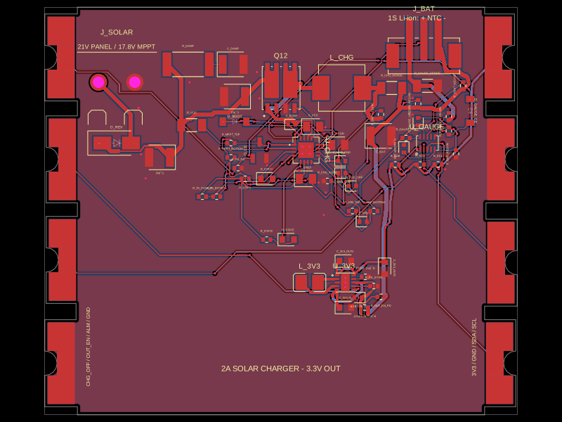 Similar packageShiboSoftwareDev/solar-battery-charger-moduleThis hardware setup integrates a solar panel, a lithium-ion battery, and a multi-rail buck converter with a battery charging IC, protection circuitry, and monitoring components, enabling solar power harvesting, battery charging, and power distribution in an embedded system.
 Discover something newimrishabh18/fitness_watchThis circuit integrates an ESP-12E microcontroller with various sensors and peripherals, including a AO3400A MOSFET for switching loads, to enable wireless control and sensor data processing.