pixalynx/pixal-gps
These files define two separate printed circuit boards: a small, two-layer battery cartridge with protection circuitry and contact pads for a pouch cell, and a larger, two-layer wireless charging dock featuring USB-C input, a resonant coil, and wireless power transmission components.
- Version
- 0.1.2
- License
- unset
- Stars
- 0
docs/design-report.md
# PIXAL GPS — design report (Rev A, 16 September 2026)

**Status: complete electrical design of three coordinated boards in tscircuit, datasheet-verified footprints and part numbers, all three boards fully routed and DRC-clean with 0 placement errors and 342 passing design assertions (see "Routing status" at the end). This is a design/prototype exercise: firmware bring-up is expected on the nRF9151 DK first, and none of the three boards has been fabricated yet.**

## 1. Product concept and architecture

A rechargeable location tracker built on the Nordic **nRF9151** SiP (LTE-M / NB-IoT / GNSS, Cortex-M33 application core, PSM/eDRX) and the Nordic **nPM1300** PMIC, with a removable battery cartridge, wireless charging and a motion-triggered wake. There is no second MCU: the nRF9151 application core runs the cellular link, GNSS, the accelerometer, the PMIC, the wireless receiver enable/monitor and server communication.

```
                 ┌────────────────────────── PCB A: tracker 34 × 24 mm, 4 layers ──────────────────────────┐
 Qi dock ─ field ─┤ Rx coil → BQ51013B (5 V) → nPM1300 VBUS ─┐                                                │
                 │                                          ├─ charger/power path → VSYS → FB1 → nRF9151 VDD  │
 Cartridge B ────┤ BAT+ ──────────────────── nPM1300 VBAT ──┘        BUCK1 1.8 V → VDD_GPIO, LIS2DW12, LNA, I²C │
 (LiPo + PCM/NTC/ID) NTC → nPM1300 NTC ; ID → AIN0                                                              │
                 │ nRF9151 ── ANT → pi-match → U.FL (LTE)     GPS ← SKY65943-11 LNA+SAW ← U.FL (GNSS) ← [AUX opt]│
                 │         ── SIM (1.8 V) → TPD3F303 → nano-SIM push-pull socket                                │
                 │         ── I²C → nPM1300 (0x6B), LIS2DW12 (0x18) ; INT1 wake ; COEX0 → LNA enable            │
                 │ SWD/RESET/UART/rails on a 2×5 pogo pad field ; SHPHLD button ; 2 status LEDs                 │
                 └──────────────────────────────────────────────────────────────────────────────────────────────┘
 PCB C: dock 56 × 44 mm, 2 layers — USB-C 5 V → IP6829 Qi BPP transmitter → A11 coil (Ø50 mm)
```

## 2. Decisions and why

| Topic | Decision | Basis (details in the linked documents) |
| --- | --- | --- |
| Modem/MCU | nRF9151-LACA-R7 (JLC C22397843) with the reference input filter, ENABLE→VDD, DEC0 4.7 µF, nRESET 1 kΩ/100 nF | Nordic PS/HDG reference BOM; [rf.md](rf.md), [power.md](power.md) |
| Antenna architecture | two U.FL connectors (LTE, GNSS) with Nordic's external LNA/SAW module on the GNSS input; the single-antenna ANT→AUX→LNA path is present but jumpered off | Nordic supports only that shared-antenna topology; DK and Thingy use two antennas; [rf.md](rf.md) |
| PMIC | nPM1300 QFN: charger, power path, BUCK1 1.8 V, LED sinks, SHPHLD button, TWI to the SiP; BUCK2/LDO2 terminated per Nordic config 3 | nPM1300 PS/HDG/reference layout; [power.md](power.md) |
| Battery | 600 mAh 503040-class cell (Honcell HCP503040NFC production, Jauch LP503040JH prototype), 5.4 × 30.5 × 40.5 mm, 1C/2C pulse | [power.md](power.md) |
| Cartridge | PCB B 26 × 7 mm: BAT+/GND/NTC/ID ENIG pads on 3 mm pitch, BQ29700 + FS8205A protection *or* JP1 bypass for a PCM'd cell; never both | [battery-pack.md](battery-pack.md) |
| Wireless | Qi BPP: TI BQ51013B receiver in the tracker (5 V out, 1 A ILIM), Injoinic IP6829 transmitter in the dock, TDK 30 mm Rx coil, A11 Tx coil | [wireless-charging.md](wireless-charging.md) |
| Motion | ST LIS2DW12, LP mode 1 at 12.5 Hz ≈ 1 µA, INT1 wake to P0.31, Zephyr driver with wake-up trigger | [firmware-pinmap.md](firmware-pinmap.md); sourcing table in `research/components.md` |
| SIM | 4FF nano-SIM push-pull socket SMN-304 (JLC C266889) + TI TPD3F303 EMI/ESD filter, 100 nF + 10 nF on SIM VCC | Nordic HDG UICC page; DK/Thingy use TPD3F303 |
| Programming | 2 × 5 pogo field at 1.27 mm: SWDIO, SWDCLK, RESET, 1V8, GND / TX, RX, VSYS, VBAT, VBUS | no USB (the nRF9151 has no USB peripheral); SWD is the only programming path |
| Stack-up | JLC04161H-7628, 1.6 mm, ENIG, 0.32 mm/0.25 mm CPWG for 50 Ω | [stackup.md](stackup.md) |
| Size | 34 × 24 mm tracker (816 mm²) | the SiP alone is 12.1 × 11.1 mm; the SIM socket 12.3 × 13.6 mm; both RF connectors, the LNA and the RF keep-outs sit on the top; PMIC, Qi, SIM, contacts and test pads on the bottom. 32 × 24 mm was tried first and abandoned when the SiP's decoupling column could not fit beside it without courtyard conflicts |

## 3. Board A layout summary

Top (component side facing the enclosure lid): nRF9151 at (−4.5, 1.0); its VDD filter column on the left edge; DEC0 and VDD_GPIO capacitors at the SiP's edge; LTE chain straight down to J1 at the bottom edge; GNSS LNA and J2 at the bottom-right; the accelerometer and its capacitors above the SiP; two LEDs and the side-actuated SHPHLD button at the top-right. Bottom: nano-SIM socket under the SiP's left half (card enters from the left edge), TPD3F303 at the bottom-left, nPM1300 with BUCK1 inductor and capacitors under the top-right, BQ51013B with its capacitor columns at the right, resonant capacitors and coil pads along the top-right edge, four battery spring contacts along the top edge, the pogo test field at the top-left. Nine ground vias sit in the SiP's centre lands (Nordic: pin 108 is the PA thermal relief) and 46 more stub vias tie every ground land to the L2 plane.

Distances that matter: LTE line 3.9 mm, GNSS input line 3.8 mm, LNA→GPS 2.9 mm (Nordic: keep short, ≤ 0.5 dB); LTE and GNSS connectors 13 mm apart with the LNA between them; the buck inductor is 20 mm from the ANT pin and on the other side of the ground plane; the Qi rectifier's noisy nodes are on the bottom under the plane.

## 4. Power, sleep and battery life

≈ 5 µA stationary floor (modem PSM 2.7 µA + PMIC 0.8 µA + accelerometer 1 µA + leakage), see [power.md](power.md); LTE-M reporting dominates: about 100 days at one fix + one report per 10 min from 600 mAh, over a year at hourly reports.

## 5. Manufacturing

JLCPCB Standard PCBA (double-sided), 4-layer JLC04161H-7628 with impedance control, ENIG 2 µin, tented 0.2/0.4 mm vias, min 0.1/0.1 mm track/space used (fab minimum 0.09). All passives are 0402/0603/0805; the smallest pitch is 0.5 mm (nRF9151 LGA, nPM1300, BQ51013B, LNA); X-ray is automatic for the LGA/QFN parts. Supply risks: nRF9151 (355 in JLC's database), nPM1300 QFN (0 at LCSC on 2026-09-14 → JLCPCB global sourcing or consignment), SKY65943-11 (46). Panelise 2 × 3 to meet the 70 × 70 mm Standard-PCBA minimum.

## 6. Routing status and remaining gates

- **Dock (C)**: fully autorouted, 0 DRC errors, netlist assertions pass.
- **Battery pack (B)**: fully hand-routed (`routingDisabled`), 0 placement/DRC errors, netlist assertions pass.
- **Tracker (A)**: fully routed, 0 placement errors, 0 DRC errors, 0 clearance findings below 0.10 mm (independent audit, `scripts/check-clearance.py`), 234 traces / 186 vias. tscircuit's own capacity autorouter never converged on this board (three full attempts each stalled at 46% of port-pathing after 30+ minutes); the copper is instead built in three explicit, source-committed stages — hand-routed RF and a handful of other constrained legs, a generated ground-plane stub mesh, and a local Freerouting 1.9 pass for the remaining signal/power nets imported back as ordinary `<trace pcbPath>` copper — plus five connections a purpose-built grid-search router placed after Freerouting still would not make in six attempts. `docs/routing.md` has the full flow, the tuning history, and why those five needed hand-routing. `bunx tsci build tracker.circuit.tsx` reproduces the routed board from source in about 20 seconds; no autorouter runs at build time.
- Design/DRC gates are closed on all three boards; nothing has been fabricated. Before ordering: run `bun run check` and `python3 scripts/check-clearance.py` after any further edit, get independent design review (RF matching, decoupling placement, thermal reliefs on the exposed pads), and confirm JLCPCB accepts the 4-layer stack-up's controlled-impedance tolerance for the 0.32/0.25 mm CPWG at quoted cost.
- Bench gates before Rev B: measure the Rx coil Ls' in the enclosure and re-pick C36/C37; run TI's FOD calibration; verify the IP6829 reel is factory-programmed; confirm VDD_GPIO power-up ordering on real hardware; conducted LTE/GNSS tests on the two connectors, then decide on the shared-antenna option; the Qi receiver's RECT capacitors sit 5-8 mm from the pin (see wireless-charging.md) and the VANT load-switch capacitor sits at the bias-T inductor rather than at LSOUT1 (see power.md) — both are placement compromises worth revisiting once the board is bench-verified.
Related Packages
 More from this authorpixalynx/esp32-gps-cellular-trackerThis code defines a hardware layout comprising a Wi-Fi-enabled ESP32 module, GPS module, cellular GSM module, battery management components (including charger, protection circuits, and voltage regulators), USB-C connector, SIM card holder, RF components, and supporting passive components for a comprehensive GPS+Cellular tracker device.
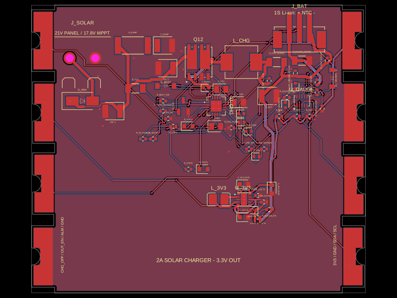 Similar packageShiboSoftwareDev/solar-battery-charger-moduleThis hardware setup integrates a solar panel, a lithium-ion battery, and a multi-rail buck converter with a battery charging IC, protection circuitry, and monitoring components, enabling solar power harvesting, battery charging, and power distribution in an embedded system.
 Discover something newimrishabh18/fitness_watchThis circuit integrates an ESP-12E microcontroller with various sensors and peripherals, including a AO3400A MOSFET for switching loads, to enable wireless control and sensor data processing.