pixalynx/nrf9151-gps-tracker
A compact 44×32 mm, 4-layer nRF9151 LTE-M/NB-IoT/GNSS tracker PCB with nPM1300 LiPo/USB-C power, nano-SIM/eSIM switching, nRF7002 Wi‑Fi scanning, accelerometer, antennas, buzzer, LEDs, SOS button, and SWD/debug connectors.
- Version
- 0.1.4
- License
- unset
- Stars
- 0
parts/Ui.tsx
import type { ChipProps } from "tscircuit"
import { pad, outline, courtyard } from "../lib/footprints"

/** Jiangsu Huawha MLT-5020 5.0 x 5.0 x 2.0 mm SMD electromagnetic buzzer (JLC C94598, 106k in stock):
 * 2-4 V (3 V rated), 100 mA max, resonant 4 kHz, 75 dB at 10 cm. Magnetic transducer = coil, so it
 * needs a square-wave drive near 4 kHz (nRF9151 PWM) through a low-side MOSFET and a flyback diode.
 * Land pattern and numbering = the JLC/EasyEDA library footprint, which matches the Huawha datasheet dimension
 * drawing (top view): pad 1 "+" bottom-left, pad 2 "-" bottom-right, pad 3 mechanical tab (NC) top-left, the
 * top-right corner is the body's chamfer and has no land. 1.7 x 0.7 mm lands on a 4.6 x 3.5 mm grid. Numbering
 * matches JLC's so the pick-and-place rotation check works. (Until 2026-09-24 the lands were numbered like a dfn4,
 * which put "+" on the mechanical tab: the buzzer would have been silent.) */
export const buzzerPins = { pin1: ["POS"], pin2: ["NEG"], pin3: ["NC"] } as const
export const Buzzer = (props: ChipProps<typeof buzzerPins>) => (
  <chip
    {...props}
    manufacturerPartNumber="MLT-5020"
    supplierPartNumbers={{ jlcpcb: ["C94598"] }}
    pinLabels={buzzerPins}
    footprint={
      <footprint>
        {pad(1, -2.3, -1.75, 1.7, 0.7)}
        {pad(2, 2.3, -1.75, 1.7, 0.7)}
        {pad(3, -2.3, 1.75, 1.7, 0.7)}
        <silkscreenpath route={[{ x: -2.5, y: 2.5 }, { x: 2.5, y: 2.5 }]} strokeWidth={0.12} />
        <silkscreenpath route={[{ x: -2.5, y: -2.5 }, { x: 2.5, y: -2.5 }]} strokeWidth={0.12} />
        <silkscreenpath route={[{ x: -2.5, y: -1.2 }, { x: -2.5, y: 1.2 }]} strokeWidth={0.12} />
        <silkscreenpath route={[{ x: 2.5, y: -1.2 }, { x: 2.5, y: 1.2 }]} strokeWidth={0.12} />
        <silkscreentext text="+" pcbX={-0.8} pcbY={-1.75} fontSize={0.8} />
        {courtyard(6.8, 5.1)}
      </footprint>
    }
    cadModel={{
      objUrl: "https://modelcdn.tscircuit.com/easyeda_models/assets/C94598.obj?uuid=5e71db11d9fa48278b90d6344e196479",
      stepUrl: "https://modelcdn.tscircuit.com/easyeda_models/assets/C94598.step?uuid=5e71db11d9fa48278b90d6344e196479",
      pcbRotationOffset: 270,
      modelOriginPosition: { x: 0, y: 0.06, z: 0 },
    }}
    schPinArrangement={{ leftSide: { direction: "top-to-bottom", pins: ["POS", "NEG"] }, rightSide: { direction: "top-to-bottom", pins: ["NC"] } }}
    pinAttributes={{ NC: { doNotConnect: true } }}
  />
)

/** Diodes Inc DMG1012T-7 N-MOSFET, SOT-523 (JLC C20512): 20 V, 630 mA, RDS(on) 500 mOhm at
 * VGS = 1.8 V, so the 1.8 V nRF9151 GPIO switches it fully. Pins 1 G, 2 S, 3 D. Footprint = the
 * EasyEDA land pattern of C20512 (0.51 x 0.40 mm lands). */
export const nmosPins = { pin1: ["G"], pin2: ["S"], pin3: ["D"] } as const
export const Dmg1012t = (props: ChipProps<typeof nmosPins>) => (
  <chip
    {...props}
    manufacturerPartNumber="DMG1012T-7"
    supplierPartNumbers={{ jlcpcb: ["C20512"] }}
    pinLabels={nmosPins}
    footprint={
      <footprint>
        {pad(3, -0.65, 0, 0.51, 0.4)}
        {pad(1, 0.65, -0.5, 0.51, 0.4)}
        {pad(2, 0.65, 0.5, 0.51, 0.4)}
        {outline(0.8, 1.6)}
        {courtyard(2.1, 2.0)}
      </footprint>
    }
    cadModel={{
      objUrl: "https://modelcdn.tscircuit.com/easyeda_models/assets/C20512.obj?uuid=3dc99d09648d4392979bbf6561129f61",
      stepUrl: "https://modelcdn.tscircuit.com/easyeda_models/assets/C20512.step?uuid=3dc99d09648d4392979bbf6561129f61",
      pcbRotationOffset: 180,
      modelOriginPosition: { x: 0, y: 0, z: -0.149 },
    }}
    schWidth={1.2}
    schHeight={1.2}
    schPinArrangement={{ leftSide: { direction: "top-to-bottom", pins: ["G"] }, topSide: { direction: "left-to-right", pins: ["D"] }, bottomSide: { direction: "left-to-right", pins: ["S"] } }}
  />
)

/** onsemi RB521S30T1G 30 V / 200 mA Schottky, SOD-523 (JLC C145179): buzzer flyback clamp.
 * EasyEDA land pattern: two 0.6 x 0.36 mm lands, 1.3 mm apart; pin 1 = cathode. */
export const schottkyPins = { pin1: ["K", "cathode"], pin2: ["A", "anode"] } as const
export const Rb521s30 = (props: ChipProps<typeof schottkyPins>) => (
  <chip
    {...props}
    manufacturerPartNumber="RB521S30T1G"
    supplierPartNumbers={{ jlcpcb: ["C145179"] }}
    pinLabels={schottkyPins}
    footprint={
      <footprint>
        {pad(1, -0.65, 0, 0.6, 0.36)}
        {pad(2, 0.65, 0, 0.6, 0.36)}
        <silkscreenpath route={[{ x: -1.1, y: -0.35 }, { x: -1.1, y: 0.35 }]} strokeWidth={0.1} />
        {courtyard(2.2, 1.0)}
      </footprint>
    }
    cadModel={{
      objUrl: "https://modelcdn.tscircuit.com/easyeda_models/assets/C145179.obj?uuid=1b4f85e18594402ead7ab158b0198846",
      stepUrl: "https://modelcdn.tscircuit.com/easyeda_models/assets/C145179.step?uuid=1b4f85e18594402ead7ab158b0198846",
      pcbRotationOffset: 180,
      modelOriginPosition: { x: -0.213, y: -0.011, z: -0.71 },
    }}
    schWidth={0.6}
    schHeight={1}
    schPinArrangement={{ topSide: { direction: "left-to-right", pins: ["K"] }, bottomSide: { direction: "left-to-right", pins: ["A"] } }}
  />
)
Related Packages
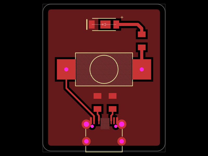 More from this authorpixalynx/usbc-led-switchA single-sided USB-C–powered LED light board with a latching pushbutton, 100 Ω current-limiting resistor, white 5730 SMD LED, and dual 5.1 kΩ USB-C CC pull-down resistors.
 Similar packageaura/diy-power-delivery-triggerThis hardware design implements a USB Type-C port with supporting power management and signal conditioning components, including a USB-C connector, a FUSB302 USB-C port controller, ESD protection diodes, a buck converter for 3.3V power regulation, an STM32 microcontroller for control and processing, an RGB LED indicator, push button, terminal block connections, and associated filtering and support components.
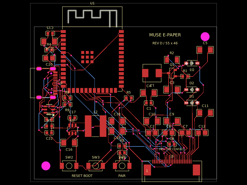 Discover something newmuse/esp32-eink-displayA 55×46 mm two-layer ESP32-S3 e-paper controller board with USB‑C power/programming, buck regulation, FPC display connector, UC8179-style boost/charge-pump circuitry, ESD protection, controls, and routed passive components.