pixalynx/nrf9151-gps-tracker
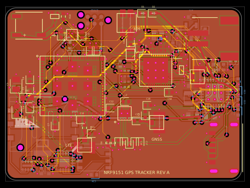
A compact 44×32 mm, 4-layer nRF9151 LTE-M/NB-IoT/GNSS tracker PCB with nPM1300 LiPo/USB-C power, nano-SIM/eSIM switching, nRF7002 Wi‑Fi scanning, accelerometer, antennas, buzzer, LEDs, SOS button, and SWD/debug connectors.
- Version
- 0.1.4
- License
- unset
- Stars
- 0
index.circuit.tsx
PCB
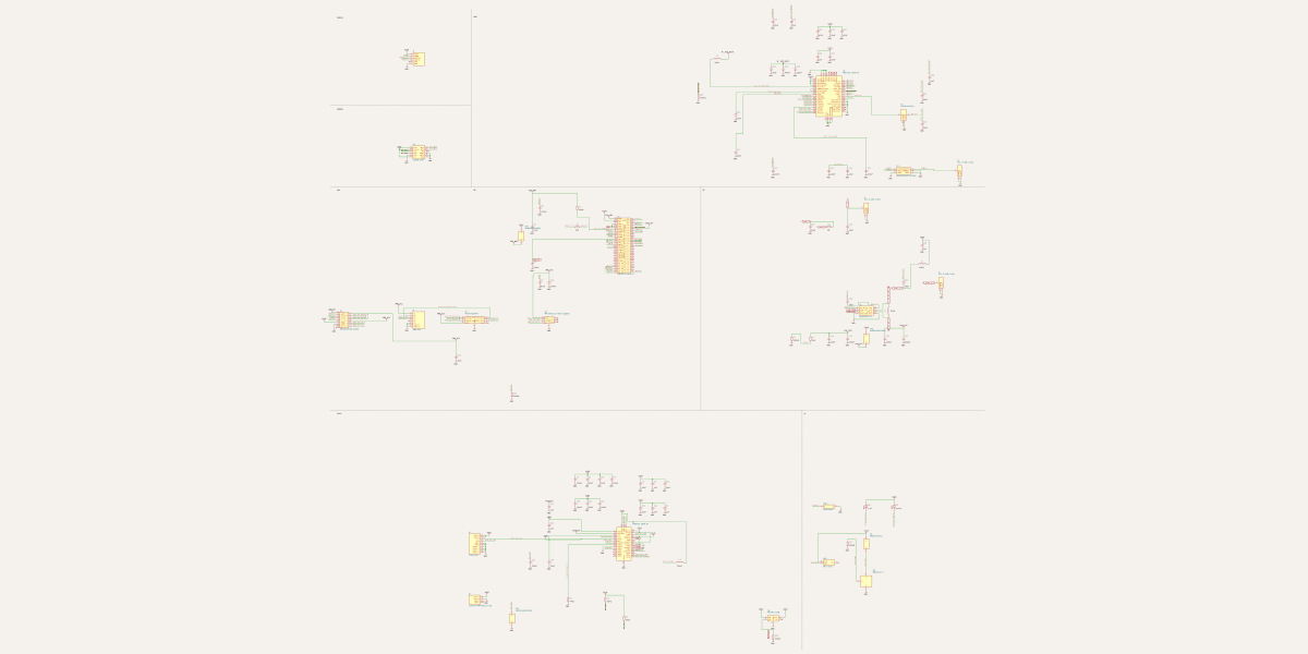
Schematic
import { Fragment } from "react"
import { nrf9151GndPins, Nrf9151 } from "./parts/Nrf9151"
import { Npm1300 } from "./parts/Npm1300"
import { Lis2dw12 } from "./parts/Lis2dw12"
import { NanoSimSocket } from "./parts/NanoSimSocket"
import { Sky65943, Tpd3f303, TactSwitch } from "./parts/RfFrontEnd"
import { Ufl, Tc2030 } from "./parts/Connectors"
import { UsbC6p, JstPh2 } from "./parts/Power"
import { Buzzer, Dmg1012t, Rb521s30 } from "./parts/Ui"
import { Nrf7002, Diplexer, Crystal40M, Rt9080, nrf7002GroundedPins } from "./parts/Wifi"
import { SimSwitch, EsimMff2 } from "./parts/Sim"
import { Cap, Res, Ind, Bead, type PassiveSpec } from "./lib/passives"
import { localPath, throughVias } from "./lib/geometry"
import { Ind0806 } from "./lib/footprints"
import { BOARD, U1, rel } from "./lib/layout"
import { GndMeshTraces, type GndMesh } from "./lib/gnd-mesh"
import { RoutedTraces, type RoutedLegs } from "./lib/routed-traces"
import routesJson from "./routing/index-routes.json"
import gndMeshJson from "./routing/index-gnd.json"

/**
 * nRF9151 GPS tracker (kids / pets), Rev A. 44 x 32 mm, 4 layers (JLC04161H-7628), double-sided assembly.
 *
 * nRF9151 SiP (LTE-M / NB-IoT / GNSS + Cortex-M33) powered by an nPM1300 PMIC from a 1-cell LiPo on a
 * JST-PH connector, charged from a USB-C (power only) receptacle. Nano-SIM socket and an MFF2 eSIM
 * share the SiP's single SIM port through an NX3DV2567 switch. nRF7002 Wi-Fi companion for SSID
 * scanning (indoor location). LIS2DW12 motion wake, SOS button on the PMIC's SHPHLD input, two
 * status LEDs on the PMIC's LED sinks, SMD buzzer for find-me. Three U.FL ports: LTE, GNSS, Wi-Fi.
 *
 * Sources for every value: docs/ and research/.
 */

// Schematic section origins (schematic units).
const S = {
  SIP: [0, 0], RF: [18, -4], SIM: [-22, -8], PWR: [0, -32], WIFI: [22, 16], MOTION: [-22, 10], UI: [22, -28], DEBUG: [-22, 20],
} as const
const sch = (sec: keyof typeof S, dx: number, dy: number): [number, number] => [S[sec][0] + dx, S[sec][1] + dy]
type P = PassiveSpec
const at = (x: number, y: number) => rel(x, y)
/** pcbX/pcbY props for a pixal-gps coordinate */
const pos = (x: number, y: number) => { const p = rel(x, y); return { pcbX: p.x, pcbY: p.y } }

// ---------------------------------------------------------------------------------------
// nRF9151 block: decoupling, LTE match and GNSS front end (pixal-gps placement, shifted)
// ---------------------------------------------------------------------------------------
const sipCaps: P[] = [
  // VDD input filter, Nordic nRF9151 reference topology (PS "Reference circuitry" + nWP056 "VDD"): C1, C2 1u and
  // C3 47u on the source (VSYS) side of FB1, C4 10u between FB1 and the VDD pin. C4 is a 10 V 0402 (Nordic allows a
  // smaller package) so it fits the slot beside FB1.B, 3.6 mm from U1.VDD. Nordic's figure calls the source-side net
  // VDD_nRF; here that net is VSYS, and VDD_NRF is the short FB1.B -> U1.VDD side.
  { name: "C1", value: "1uF", footprint: "0603", ...at(-14.9, -3.6), rot: 90, sch: sch("PWR", 3.1, 6.4), section: "PWR", schRot: 270 },
  { name: "C2", value: "1uF", ...at(-12.45, 0.5), rot: 90, sch: sch("PWR", 4.4, 3.8), section: "PWR", schRot: 270 },
  { name: "C3", value: "47uF", footprint: "0805", ...at(-15.0, 1.3), rot: 90, sch: sch("PWR", 1.8, 6.4), section: "PWR", schRot: 270 },
  { name: "C4", value: "10uF", jlc: "C408132", ...at(-12.45, -3.0), rot: 90, sch: sch("SIP", -9.8, 2), section: "SIP", schRot: 270 },
  { name: "C5", value: "100nF", ...at(-0.1, 7.7), rot: 90, sch: sch("PWR", -5.2, 6.9), section: "PWR", schRot: 270 },
  { name: "C6", value: "4.7uF", ...at(-1.2, 7.7), rot: 90, sch: sch("PWR", -3.9, 6.9), section: "PWR", schRot: 270 },
  { name: "C7", value: "4.7uF", ...at(-7.75, -6.2), rot: 90, sch: sch("SIP", -9.0, -4), section: "SIP", schRot: 90 }, // DEC0: exactly 4.7 uF
  { name: "C8", value: "100nF", ...at(-12.45, 2.4), rot: 90, sch: sch("SIP", -9.0, 4), section: "SIP", schRot: 270 }, // nRESET
  { name: "C9", value: "100nF", ...at(-12.45, -5.2), rot: 90, sch: sch("SIP", -9.8, -2), section: "SIP", schRot: 90 }, // SIM_1V8
  // LTE match reservation: shunt (DNP) - series 0R - shunt (DNP)
  { name: "C10", value: "22pF", ...at(-2.75, -5.3), rot: 0, sch: sch("RF", 2, 6), section: "RF", schRot: 90, dnp: true },
  { name: "C11", value: "22pF", ...at(-0.75, -7.85), rot: 0, sch: sch("RF", 6, 6), section: "RF", schRot: 270, dnp: true },
  // GNSS front end (SKY65943-11, Nordic DK values)
  { name: "C12", value: "39pF", ...at(2.75, -3.1), rot: 0, sch: sch("RF", 6, -2), section: "RF", schOrientation: "vertical" },
  { name: "C13", value: "39pF", ...at(7.6, -5.5), rot: 0, sch: sch("RF", 12, 0), section: "RF", schOrientation: "vertical" },
  { name: "C14", value: "100nF", ...at(4.1, -9.6), rot: 270, sch: sch("RF", 4, -6), section: "RF", schRot: 270 },
  { name: "C15", value: "100pF", ...at(5.1, -9.6), rot: 270, sch: sch("RF", 6, -6), section: "RF", schRot: 270 },
  { name: "C16", value: "100nF", ...at(7.1, -9.6), rot: 270, sch: sch("RF", 10, -6), section: "RF", schRot: 270 },
  { name: "C17", value: "100pF", ...at(8.1, -9.6), rot: 270, sch: sch("RF", 12, -6), section: "RF", schRot: 270 },
  { name: "C18", value: "1uF", ...at(9.6, -2.6), rot: 0, sch: sch("RF", 14, 4), section: "RF", schRot: 270 }, // VANT (LSOUT1) at the bias-T
]
const sipRes: P[] = [
  { name: "R1", value: "10k", ...at(-5.0, 9.6), rot: 90, side: "bottom", sch: sch("SIP", -5, 4), section: "SIP", schRot: 270 }, // ENABLE -> VDD
  { name: "R2", value: "1k", ...at(-5.0, 7.5), rot: 90, side: "bottom", sch: sch("SIP", -5, 2), section: "SIP" }, // nRESET series
  { name: "R3", value: "0", ...at(-2.25, -6.8), rot: 90, sch: sch("RF", 4, 6), section: "RF" }, // LTE series element
  { name: "R4", value: "1k", ...at(3.1, -9.6), rot: 90, sch: sch("RF", 2, -6), section: "RF", schRot: 90 }, // COEX0 -> VEN
  { name: "R5", value: "100k", ...at(2.1, -9.6), rot: 270, sch: sch("RF", 0, -6), section: "RF", schRot: 270 }, // COEX0 pull-down
]
const sipInd: P[] = [
  { name: "L2", value: "9.1nH", ...at(5.45, -1.9), rot: 0, sch: sch("RF", 10.4, -3), section: "RF", schRot: 90 },
  { name: "L3", value: "68nH", ...at(9.05, -4.3), rot: 90, sch: sch("RF", 14, 2), section: "RF", dnp: true }, // active-antenna bias-T
]

// ---------------------------------------------------------------------------------------
// Power (nPM1300), user interface, motion sensor, SIM socket
// ---------------------------------------------------------------------------------------
const PMIC = { x: 17.0, y: 0.2 } // bottom side, rotated 180: VBUS/VBAT/CC column faces the right edge
const pwrCaps: P[] = [
  { name: "C20", value: "2.2uF", x: 21.35, y: 0.4, rot: 90, side: "bottom", sch: sch("PWR", -8, -2), section: "PWR", schRot: 270 }, // VBAT
  { name: "C21", value: "10uF", footprint: "0603", x: 16.2, y: -4.25, rot: 180, side: "bottom", sch: sch("PWR", 4.4, 6.4), section: "PWR", schRot: 270 }, // VSYS, + land under VOUT2 (=VSYS)
  { name: "C22", value: "1uF", x: 21.35, y: -1.5, rot: 90, side: "bottom", sch: sch("PWR", -8, 2), section: "PWR", schRot: 270 }, // VBUS
  { name: "C23", value: "1uF", x: 21.35, y: -3.4, rot: 90, side: "bottom", sch: sch("PWR", -8, 4), section: "PWR", schRot: 270 }, // VBUSOUT (mandatory)
  { name: "C24", value: "10uF", footprint: "0603", x: 12.3, y: 2.35, rot: 90, side: "bottom", sch: sch("PWR", 1.8, 3.8), section: "PWR", schRot: 270 }, // PVDD
  { name: "C26", value: "10uF", footprint: "0603", x: 12.9, y: -3.9, rot: 0, side: "bottom", sch: sch("PWR", -2.6, 6.9), section: "PWR", schRot: 270 }, // VOUT1 1.8 V
  { name: "C27", value: "100nF", x: 16.75, y: 5.0, rot: 270, side: "bottom", sch: sch("PWR", -1.3, 6.9), section: "PWR", schRot: 270 }, // VDDIO
  { name: "C29", value: "100pF", x: 18.65, y: 5.0, rot: 90, side: "bottom", sch: sch("PWR", -10, -2), section: "PWR", schRot: 270 }, // NTC pin filter (<= 100 pF)
  // LIS2DW12
  { name: "C30", value: "100nF", x: -11.6, y: 11.0, rot: 90, sch: sch("PWR", -5.2, 4.3), section: "PWR", schRot: 270 }, // VDD_IO
  { name: "C31", value: "10uF", x: -7.7, y: 11.0, rot: 90, sch: sch("PWR", -3.9, 4.3), section: "PWR", schRot: 270 }, // VDD
  // nano-SIM VCC at the socket (DK C48)
  { name: "C32", value: "10nF", x: -20.0, y: 1.2, rot: 0, side: "bottom", sch: sch("SIM", 4, -4), section: "SIM", schRot: 270 },
]
const pwrRes: P[] = [
  { name: "R6", value: "47k", x: 21.35, y: 2.3, rot: 90, side: "bottom", sch: sch("PWR", -6, -6), section: "PWR", schRot: 270 }, // VSET1 = 1.8 V
  { name: "R8", value: "10k", x: 17.7, y: 5.0, rot: 90, side: "bottom", sch: sch("PWR", -2, -6), section: "PWR", schRot: 90 }, // SDA pull-up
  { name: "R9", value: "10k", x: 15.8, y: 5.0, rot: 90, side: "bottom", sch: sch("PWR", 0, -8), section: "PWR", schRot: 90 }, // SCL pull-up
  { name: "R10", value: "100k", x: -11.2, y: 14.4, rot: 90, sch: sch("UI", 2, -4), section: "UI", schRot: 270 }, // buzzer gate pull-down
]
const pwrInd: P[] = [
  { name: "L1", value: "2.2uH", footprint: <Ind0806 />, fpKey: "0806", x: 12.1, y: -0.8, rot: 90, side: "bottom", sch: sch("PWR", 6, -2), section: "PWR" }, // BUCK1
]
// ---------------------------------------------------------------------------------------
// Wi-Fi locating: nRF7002 (Nordic reference schematic, PS v1.2 figure 19; C41..C58 = Nordic C1..C18)
// ---------------------------------------------------------------------------------------
export const U5 = { x: 6.0, y: 4.4 } // nRF7002 centre (top), rotated 90: RF pins (1-12) face +x, XO/LDO pins (13-24) +y,
// buck pins (25-36) -x, SPI (37-38, 35-36) and HOST_IRQ toward the SiP at the lower left.
const wifiCaps: P[] = [
  // buck side (left)
  { name: "C41", value: "4.7uF", x: 2.95, y: 8.75, rot: 90, sch: sch("WIFI", -1.2, 6.9), section: "WIFI", schRot: 270 }, // BUCKVBAT (25)
  { name: "C42", value: "4.7uF", x: 1.3, y: 9.75, rot: 90, sch: sch("WIFI", -6.2, 2.9), section: "WIFI", schRot: 270 }, // VDD_BUCK at L5
  { name: "C48", value: "10nF", footprint: "0201", x: 2.1, y: 5.2, rot: 90, sch: sch("WIFI", -10, -2), section: "WIFI", schRot: 270 }, // BUCKVMID (29); its ground end ties to BUCKVSS (28)
  { name: "C47", value: "2.2uF", footprint: "0201", x: 0.6, y: 1.3, rot: 0, side: "bottom", sch: sch("WIFI", 0.1, 6.9), section: "WIFI", schRot: 270 }, // BUCKVBATS (31)
  { name: "C44", value: "470nF", footprint: "0201", x: 0.6, y: 4.3, rot: 0, side: "bottom", sch: sch("WIFI", -4.9, 2.9), section: "WIFI", schRot: 270 }, // PWRBUCKVDD (32, land y=3.8: caps follow the land order so the escapes don't cross)
  { name: "C50", value: "1uF", footprint: "0201", x: 0.6, y: 3.3, rot: 0, side: "bottom", sch: sch("WIFI", -4, 8), section: "WIFI", schRot: 270 }, // DIGVDD (33)
  { name: "C49", value: "2.2uF", footprint: "0201", x: 0.6, y: 2.3, rot: 0, side: "bottom", sch: sch("WIFI", -6, 8), section: "WIFI", schRot: 270 }, // PWRIOVDD (34, land y=3.0)
  // XO / LDO side (top)
  { name: "C55", value: "2.2uF", footprint: "0201", x: 7.0, y: 8.45, rot: 90, sch: sch("WIFI", 10, 0), section: "WIFI", schRot: 270 }, // XOLDO (16)
  { name: "C43", value: "220nF", footprint: "0201", x: 7.4, y: 10.3, rot: 90, sch: sch("WIFI", -3.6, 2.9), section: "WIFI", schRot: 270 }, // RFBUCKVDD (15), at the top of the pin-15 channel
  { name: "C53", value: "22nF", footprint: "0201", x: 7.8, y: 8.45, rot: 90, sch: sch("WIFI", 10, -3), section: "WIFI", schRot: 270 }, // RFVDD (14), straight above the pin
  { name: "C46", value: "4.7uF", x: 9.2, y: 9.0, rot: 90, side: "bottom", sch: sch("WIFI", 1.4, 6.9), section: "WIFI", schRot: 270 }, // VBAT (13), bottom as in Nordic's layout
  { name: "C56", value: "1uF", footprint: "0201", x: 5.8, y: 8.45, rot: 90, sch: sch("WIFI", 10.8, 2), section: "WIFI", schRot: 270 }, // AFELDO (19)
  { name: "C45", value: "1uF", footprint: "0201", x: 5.0, y: 8.45, rot: 90, sch: sch("WIFI", -1.2, 4.3), section: "WIFI", schRot: 270 }, // AFEVBAT (20)
  // RF side (right)
  { name: "C52", value: "100nF", footprint: "0201", x: 10.1, y: 5.85, rot: 0, sch: sch("WIFI", 0, -8), section: "WIFI", schRot: 270 }, // PAVDD0 (10)
  { name: "C54", value: "470nF", footprint: "0201", x: 10.9, y: 6.45, rot: 0, sch: sch("WIFI", 4, -8), section: "WIFI", schRot: 270 }, // SXLDO (11)
  { name: "C51", value: "4.7uF", x: 10.35, y: 7.3, rot: 0, sch: sch("WIFI", 2, -8), section: "WIFI", schRot: 270 }, // PALDO / PAVDD (12, 10, 8)
  { name: "C57", value: "100nF", footprint: "0201", x: 10.3, y: 2.2, rot: 0, sch: sch("WIFI", -6, -8), section: "WIFI", schRot: 270 }, // OTPVDD (1)
  // host side (bottom)
  { name: "C58", value: "2.2uF", x: 8.6, y: 0.3, rot: 0, sch: sch("WIFI", -10, -6), section: "WIFI", schRot: 270 }, // IOVDD (48)
  // RT9080 3.3 V LDO (Wi-Fi VBAT, buzzer, antenna bias)
  { name: "C59", value: "1uF", x: 15.2, y: 11.6, rot: 90, side: "bottom", sch: sch("PWR", 3.1, 3.8), section: "PWR", schRot: 270 }, // LDO VIN
  { name: "C60", value: "2.2uF", x: 10.0, y: 11.6, rot: 90, side: "bottom", sch: sch("WIFI", 0.1, 4.3), section: "WIFI", schRot: 270 }, // LDO VOUT
  // SIM switch / eSIM supplies
  { name: "C33", value: "100nF", x: -13.9, y: -14.3, rot: 90, side: "bottom", sch: sch("PWR", -2.6, 4.3), section: "PWR", schRot: 270 }, // switch VCC
  { name: "C34", value: "100nF", x: -5.5, y: -15.0, rot: 0, side: "bottom", sch: sch("SIM", 14, 4), section: "SIM", schRot: 270 }, // eSIM VCC
]
const wifiRes: P[] = [
  { name: "R11", value: "100k", x: -15.3, y: -14.3, rot: 90, side: "bottom", sch: sch("SIM", 10, -8), section: "SIM", schRot: 270 }, // SIM_SEL pull-down: nano-SIM by default
  { name: "R12", value: "100k", x: -0.6, y: 5.6, rot: 90, side: "bottom", sch: sch("WIFI", -14, 0), section: "WIFI", schRot: 270 }, // BUCKEN pull-down
  { name: "R13", value: "100k", x: 12.6, y: 14.3, rot: 0, side: "bottom", sch: sch("PWR", 16, -10), section: "PWR", schRot: 270 }, // LDO EN pull-down
]
const wifiInd: P[] = [
  { name: "L5", value: "3.3uH", footprint: <Ind0806 />, fpKey: "0806", jlc: "C50325850", x: 1.3, y: 7.35, rot: 90, sch: sch("WIFI", -12, 4), section: "WIFI" }, // nRF7002 buck (APLH2016-3R3M, 1.25 A, 250 mOhm)
]
// ---------------------------------------------------------------------------------------
// Grounds: every land on the GND net is declared (internally bonded groups do not give the
// other pins a net), see the memory note in docs/design.md.
// ---------------------------------------------------------------------------------------
const GND_LANDS: string[] = [
  ...nrf9151GndPins.map((p) => `U1.${p}`),
  "U2.GND1", "U2.GND2", "U2.GND3", "U2.GND4", "U2.GND_PAD",
  "J1.GND1", "J1.GND2", "J2.GND1", "J2.GND2",
  "C1.pin2", "C2.pin2", "C3.pin2", "C4.pin2", "C5.pin2", "C6.pin2", "C7.pin1", "C8.pin2", "C9.pin1", "C10.pin1", "C11.pin2",
  "C14.pin2", "C15.pin2", "C16.pin2", "C17.pin2", "C18.pin2", "R5.pin2",
  // nPM1300: paddle + power grounds
  "U3.AVSS", "U3.PVSS1", "U3.PVSS2",
  "C20.pin2", "C21.pin2", "C22.pin2", "C23.pin2", "C24.pin2", "C26.pin2", "C27.pin2", "C29.pin2",
  "J5.GND1", "J5.GND2", "J5.SHELL1", "J5.SHELL2", "J5.SHELL3", "J5.SHELL4", "J6.BAT_N", "SW1.B", "SW1.B2", "Q1.S", "R10.pin2", "RT1.B",
  "U6.GND1", "U6.GND2", "U6.SDO", "U6.RES", "C30.pin2", "C31.pin2",
  "J4.SHELL1", "J4.SHELL2", "J4.GND", "U4.GND", "C32.pin2", "J7.GND",
  // Wi-Fi block, LDO, SIM switch, eSIM
  "U5.VSS", "U5.EP", "U5.BUCKVSS1", "U5.BUCKVSS2", ...nrf7002GroundedPins.map((p) => `U5.${p}`), "FL1.GND1", "FL1.GND2", "FL1.GND3", "J3.GND1", "J3.GND2", "X1.GND1", "X1.GND2",
  ...["C41", "C42", "C43", "C44", "C45", "C46", "C47", "C48", "C49", "C50", "C51", "C52", "C53", "C54", "C55", "C56", "C57", "C58", "C59", "C60", "C33", "C34"].map((c) => `${c}.pin2`),
  "U9.GND", "R11.pin2", "R12.pin2", "R13.pin2", "U7.GND", "U7.EP", "U8.GND",
]

// The native autorouter is opt-in: KT_AUTOROUTE=1 npx tsci build index.circuit.tsx
const nativeAutoroute = typeof process !== "undefined" && process.env?.KT_AUTOROUTE === "1"

export default () => (
  <board width={BOARD.w} height={BOARD.h} layers={4} thickness={1.6} borderRadius={2} routingDisabled={!nativeAutoroute}
    title="nRF9151 GPS tracker / nRF9151 + nRF7002 + nPM1300 / Rev A"
    fabricatorPreset="jlcpcb_standard"
    minTraceWidth={0.1} minTraceToPadEdgeClearance={0.1} minPadEdgeToPadEdgeClearance={0.1}
    minViaHoleDiameter={0.2} minViaPadDiameter={0.4} minBoardEdgeClearance={0.3}
    pcbStyle={{ viaHoleDiameter: "0.2mm", viaPadDiameter: "0.4mm" }}
    defaultTraceWidth={0.15} doubleSidedAssembly
  >
    {/* router works to wider clearances than the 0.1 mm DRC floor: it lands ~0.05 mm short in dense spots */}
    <autoroutingphase minTraceToPadEdgeClearance="0.16mm" minViaEdgeToPadEdgeClearance="0.2mm" />
    {Object.keys(S).map((name) => <Fragment key={name}><schematicsection name={name} displayName={name} /></Fragment>)}

    <net name="GND" isGroundNet />
    <net name="VSYS" isPowerNet nominalTraceWidth={0.4} />
    <net name="VBAT" isPowerNet nominalTraceWidth={0.4} />
    <net name="VBUS" isPowerNet nominalTraceWidth={0.4} />
    <net name="V1V8" isPowerNet nominalTraceWidth={0.25} />
    <net name="V3V3" isPowerNet nominalTraceWidth={0.3} />
    <net name="VDD_NRF" isPowerNet nominalTraceWidth={0.4} />

    {/* ----------------------------- nRF9151 SiP ----------------------------- */}
    <Nrf9151 name="U1" pcbX={U1.x} pcbY={U1.y} schX={S.SIP[0]} schY={S.SIP[1]} schSectionName="SIP" />
    <Bead name="FB1" value="22R" mpn="BLM18SD220SN1D" jlc="C710389" {...at(-12.9, -1.25)} rot={0} sch={sch("SIP", -11, 1)} section="SIP" />
    <trace from="FB1.A" to="net.VSYS" /><trace from="FB1.B" to="net.VDD_NRF" />
    <trace from="U1.VDD" to="net.VDD_NRF" />
    <trace from="C1.pin1" to="net.VSYS" /><trace from="C2.pin1" to="net.VSYS" />
    <trace from="C3.pin1" to="net.VSYS" /><trace from="C4.pin1" to="net.VDD_NRF" />
    <trace from="R1.pin1" to="net.VDD_NRF" /><trace from="R1.pin2" to="U1.ENABLE" />
    <trace from="U1.VDD_GPIO" to="net.V1V8" /><trace from="C5.pin1" to="net.V1V8" /><trace from="C6.pin1" to="net.V1V8" />
    <trace from="U1.DEC0" to="net.DEC0" /><trace from="C7.pin2" to="net.DEC0" />
    <trace from="U1.nRESET" to="net.NRESET" /><trace from="C8.pin1" to="net.NRESET" />
    <trace from="R2.pin2" to="net.NRESET" /><trace from="R2.pin1" to="net.RESET_TP" />
    <trace from="U1.SWDIO" to="net.SWDIO" /><trace from="U1.SWDCLK" to="net.SWDCLK" />
    <trace from="U1.SIM_1V8" to="net.SIM_1V8" /><trace from="C9.pin2" to="net.SIM_1V8" />
    <trace from="U1.SIM_RST" to="net.SIM_RST" /><trace from="U1.SIM_CLK" to="net.SIM_CLK" /><trace from="U1.SIM_IO" to="net.SIM_IO" />

    {/* ----------------------------- LTE antenna path ----------------------------- */}
    <Ufl name="J1" {...pos(-2.25, -10.0)} pcbRotation={180} schX={S.RF[0] + 8} schY={S.RF[1] + 8} schSectionName="RF" />
    <trace name="rf_ant_1" from="U1.ANT" to="C10.pin2" thickness={0.32} pcbPath={[]} />
    <trace name="rf_ant_2" from="C10.pin2" to="R3.pin2" thickness={0.32} pcbPath={[]} />
    <trace name="rf_ant_3" from="R3.pin1" to="J1.SIG" thickness={0.32} pcbPath={[]} />
    <trace name="rf_ant_4" from="C11.pin1" to="R3.pin1" thickness={0.32} pcbPath={localPath([at(-2.25, -7.85)], at(-0.75, -7.85), 0)} />

    {/* ----------------------------- GNSS front end ----------------------------- */}
    <Sky65943 name="U2" {...pos(5.2, -4.1)} schX={S.RF[0] + 8} schY={S.RF[1] - 3} schSectionName="RF" />
    <Ufl name="J2" {...pos(11.2, -5.8)} pcbRotation={270} schX={S.RF[0] + 16} schY={S.RF[1]} schSectionName="RF" />
    <trace name="rf_gps_1" from="U1.GPS" to="C12.pin1" thickness={0.32} pcbPath={[]} />
    <trace name="rf_gps_2" from="C12.pin2" to="U2.RF_OUT" thickness={0.32} pcbPath={[]} />
    <trace from="U2.AMP_IN" to="L2.pin1" /><trace from="U2.FILT_OUT" to="L2.pin2" />
    <trace name="rf_gnss_in_1" from="U2.RF_IN" to="C13.pin1" thickness={0.32} pcbPath={[]} />
    <trace name="rf_gnss_in_2" from="C13.pin2" to="J2.SIG" thickness={0.32} pcbPath={[]} />
    <trace name="rf_bias_stub" from="L3.pin1" to="J2.SIG" thickness={0.25} pcbPath={localPath([at(9.05, -5.638)], at(9.05, -4.3), 90)} />
    <trace from="L3.pin2" to="net.VANT" /><trace from="C18.pin1" to="net.VANT" />
    <trace name="lna_gnd2" from="U2.GND2" to="U2.GND_PAD" thickness={0.25} pcbPath={localPath([at(5.7, -4.6)], at(5.2, -4.1), 0)} />
    <trace name="lna_gnd3" from="U2.GND3" to="U2.GND_PAD" thickness={0.25} pcbPath={localPath([at(6.0, -3.6)], at(5.2, -4.1), 0)} />
    <trace name="lna_gnd4" from="U2.GND4" to="U2.GND_PAD" thickness={0.25} pcbPath={localPath([at(4.7, -3.8)], at(5.2, -4.1), 0)} />
    {/* LNA enable from COEX0 (modem drives it high while GNSS receives); 100k pull-down mandatory */}
    <trace from="U1.COEX0" to="net.COEX0" /><trace from="R5.pin1" to="net.COEX0" />
    <trace from="R4.pin1" to="net.COEX0" /><trace from="R4.pin2" to="net.LNA_VEN" />
    <trace from="U2.VEN" to="net.LNA_VEN" /><trace from="C14.pin1" to="net.LNA_VEN" /><trace from="C15.pin1" to="net.LNA_VEN" />
    <Bead name="FB2" value="120R" mpn="BLM15AG121SN1D" jlc="C85812" footprint="0402" {...at(6.1, -9.6)} rot={90} sch={sch("RF", 8, -6)} section="RF" />
    <trace from="FB2.A" to="net.V1V8" /><trace from="FB2.B" to="net.LNA_VCC" />
    <trace from="U2.VCC" to="net.LNA_VCC" /><trace from="C16.pin1" to="net.LNA_VCC" /><trace from="C17.pin1" to="net.LNA_VCC" />

    {/* ----------------------------- nPM1300 power management ----------------------------- */}
    <Npm1300 name="U3" pcbX={PMIC.x} pcbY={PMIC.y} pcbRotation={180} layer="bottom" schX={S.PWR[0]} schY={S.PWR[1]} schSectionName="PWR" />
    {/* USB-C (power only): VBUS and the CC pins go straight to the PMIC (internal 5.1k Rd) */}
    <UsbC6p name="J5" pcbX={18.3} pcbY={-10.0} pcbRotation={90} schX={S.PWR[0] - 16} schY={S.PWR[1]} schSectionName="PWR" />
    <trace from="J5.VBUS1" to="net.VBUS" /><trace from="J5.VBUS2" to="net.VBUS" />
    <trace from="J5.CC1" to="U3.CC1" /><trace from="J5.CC2" to="U3.CC2" />
    <trace from="U3.VBUS" to="net.VBUS" /><trace from="C22.pin1" to="net.VBUS" />
    <trace from="U3.VBUSOUT" to="net.VBUSOUT" /><trace from="C23.pin1" to="net.VBUSOUT" />
    {/* LiPo on JST-PH (pin 1 = BAT+) with an on-board 10k NTC for JEITA charge limits */}
    <JstPh2 name="J6" pcbX={13.9} pcbY={10.3} pcbRotation={90} schX={S.PWR[0] - 16} schY={S.PWR[1] - 6} schSectionName="PWR" />
    <trace from="J6.BAT_P" to="net.VBAT" />
    <trace from="U3.VBAT" to="net.VBAT" /><trace from="C20.pin1" to="net.VBAT" />
    <chip name="RT1" manufacturerPartNumber="NCP15XH103F03RC" supplierPartNumbers={{ jlcpcb: ["C77131"] }} footprint="0402"
      pcbX={20.4} pcbY={6.2} pcbRotation={0} layer="bottom" pinLabels={{ pin1: ["A"], pin2: ["B"] }}
      schX={S.PWR[0] - 12} schY={S.PWR[1] - 8} schSectionName="PWR" schWidth={0.6} schHeight={1}
      schPinArrangement={{ topSide: { direction: "left-to-right", pins: ["A"] }, bottomSide: { direction: "left-to-right", pins: ["B"] } }} />
    <trace from="U3.NTC" to="net.BAT_NTC" /><trace from="RT1.A" to="net.BAT_NTC" /><trace from="C29.pin1" to="net.BAT_NTC" />
    <trace from="U3.VSYS" to="net.VSYS" /><trace from="C21.pin1" to="net.VSYS" />
    <trace from="U3.PVDD" to="net.VSYS" /><trace from="C24.pin1" to="net.VSYS" />
    {/* BUCK1 = 1.8 V (VSET1 47k): VDD_GPIO, sensors, LNA, nRF7002 IOVDD, SIM switch */}
    <trace from="U3.SW1" to="L1.pin1" /><trace from="L1.pin2" to="net.V1V8" /><trace from="U3.VOUT1" to="net.V1V8" />
    <trace from="C26.pin1" to="net.V1V8" /><trace from="U3.VSET1" to="R6.pin1" /><trace from="R6.pin2" to="net.GND" />
    {/* BUCK2 unused (Nordic reference config 3): VSET2 and PVSS2 to GND, VOUT2 tied to VSYS, SW2 open. Its 200 mA
        limit is below the nRF7002's TX peak, so the 3.3 V rail comes from the RT9080 LDO (U9) instead. */}
    <trace from="U3.VOUT2" to="net.VSYS" /><trace from="U3.VSET2" to="net.GND" />
    {/* Load switch 1: V3V3 -> active GNSS antenna bias (off unless an active antenna is fitted).
        Load switch 2: V1V8 -> nRF7002 IOVDD, switched by the Wi-Fi driver (iovdd-regulator = LDSW2). */}
    <trace from="U3.LSIN1" to="net.V3V3" /><trace from="U3.LSOUT1" to="net.VANT" />
    <trace from="U3.LSIN2" to="net.V1V8" /><trace from="U3.LSOUT2" to="net.WIFI_IOVDD" />
    <trace from="U3.VDDIO" to="net.V1V8" /><trace from="C27.pin1" to="net.V1V8" />
    {/* The via-filled centre pads (AVSS, nRF7002 EP, switch EP) are never router endpoints (the router aborts on them):
        each is tied to an adjacent ground pin by a short fixed trace, and the ground mesh / router serve that pin. */}
    {/* the nPM1300 right-hand pins (VBAT, VSYS, VBUS, VBUSOUT at 0.5 mm pitch) face their caps C20/C22/C23 at the board
        edge; whichever pin Freerouting took last got boxed in, so the corner is laid by hand: VBAT straight into C20,
        VSYS onto a via, VBUS dog-leg into C22, VBUSOUT down on inner2 to C23. VDDIO straight up into C27. */}
    <trace name="pmic_vbat_cap" from="U3.VBAT" to="C20.pin1" thickness={0.3} pcbPath={[]} />
    {/* battery feed: JST pin 1 -> C20 at nPM1300 VBAT, 0.4 mm on top (laid before the router; on inner2 it walled off the
        PMIC's LED/I2C escapes, as a 0.3 mm router net it found no way out of the PMIC corner). scripts/hand-route-net.py */}
    <trace name="pwr_vbat_feed" from="C20.pin1" to="J6.BAT_P" thickness={0.4} pcbPath={throughVias([{ x: 0.51, y: 0.0 }, { x: 0.0857, y: 0.4243, via: true, toLayer: "top" }, { x: 0.5857, y: 0.85 }, { x: 1.6857, y: 2.95 }, { x: 1.6857, y: 3.55 }, { x: 2.8857, y: 4.75 }, { x: 5.6857, y: 6.05 }, { x: 8.9, y: 7.45 }])} />
    <trace name="pmic_vsys_esc" from="U3.VSYS" to="net.VSYS" thickness={0.3} pcbPath={localPath([{ x: 20.25, y: 0.45 }, { x: 20.25, y: 0.45, via: true, toLayer: "inner2" }], PMIC, 180)} />
    <trace name="pmic_vbus_cap" from="U3.VBUS" to="C22.pin1" thickness={0.15} pcbPath={localPath([{ x: 20.35, y: -0.05 }, { x: 21.1, y: -0.8 }], PMIC, 180)} />
    <trace name="pmic_vbusout_cap" from="U3.VBUSOUT" to="C23.pin1" thickness={0.15} pcbPath={localPath([{ x: 20.25, y: -0.6, via: true, toLayer: "inner2" }, { x: 20.6, y: -2.89, via: true, toLayer: "bottom" }], PMIC, 180)} />
    <trace name="pmic_vddio_cap" from="U3.VDDIO" to="C27.pin1" thickness={0.15} pcbPath={[]} />
    {/* load-switch escapes of the nPM1300 bottom pin row, staggered vias (0.5 mm pitch leaves no room for a via per
        pin in one row); Freerouting otherwise dropped LSOUT1's via under LSIN1 and left LSIN1 unrouted */}
    <trace name="pmic_lsin2_esc" from="U3.LSIN2" to="net.V1V8" thickness={0.15} pcbPath={localPath([{ x: 16.25, y: -3.0 }, { x: 16.25, y: -3.0, via: true, toLayer: "inner2" }], PMIC, 180)} />
    <trace name="pmic_lsout1_esc" from="U3.LSOUT1" to="net.VANT" thickness={0.1} pcbPath={localPath([{ x: 16.75, y: -3.47 }, { x: 16.75, y: -3.47, via: true, toLayer: "inner2" }], PMIC, 180)} />
    <trace name="pmic_lsin1_esc" from="U3.LSIN1" to="net.V3V3" thickness={0.15} pcbPath={localPath([{ x: 17.25, y: -3.0 }, { x: 17.25, y: -3.0, via: true, toLayer: "inner2" }], PMIC, 180)} />
    <trace name="pmic_avss_tie" from="U3.AVSS" to="U3.PVSS2" thickness={0.2} pcbPath={localPath([{ x: 15.25, y: 0.95 }], PMIC, 180)} />
    {/* I2C fan-outs of the nPM1300 top pin row, fixed before the router runs: the row has ~1.1 mm to the pull-up/VDDIO
        passives, Freerouting kept giving the only via spots to SHPHLD and left SDA or SCL unrouted. SDA climbs on top,
        SCL on inner2, so the V1V8 link along the R9-C27-R8 row stays free. */}
    <trace name="pmic_sda_fanout" from="U3.SDA" to="R8.pin1" thickness={0.1} pcbPath={localPath([{ x: 17.2, y: 3.42, via: true, toLayer: "top" }, { x: 17.2, y: 6.35 }, { x: 17.7, y: 6.35, via: true, toLayer: "bottom" }], PMIC, 180)} />
    <trace name="pmic_scl_fanout" from="U3.SCL" to="R9.pin1" thickness={0.1} pcbPath={localPath([{ x: 17.75, y: 3.39, via: true, toLayer: "inner2" }, { x: 15.8, y: 5.34 }, { x: 15.8, y: 6.3, via: true, toLayer: "bottom" }], PMIC, 180)} />
    {/* The right-hand PMIC capacitor column sits between the PMIC's escape lanes and the board edge: each ground land
        gets a plane via at its outer (edge-side) end, 0.32 mm from the edge. */}
    {[["C20", 0.4, -0.11], ["C22", -1.5, -2.01], ["R6", 2.3, 1.79]].map(([ref, cy, gy]) => (
      <Fragment key={`edgevia-${ref}`}>
        <trace name={`gvia_${ref}`} from={`${ref}.pin2`} to="net.GND" thickness={0.2}
          pcbPath={localPath([{ x: 21.48, y: gy as number }, { x: 21.48, y: gy as number, via: true, toLayer: "inner1" }], { x: 21.35, y: cy as number }, 90)} />
      </Fragment>
    ))}
    <trace from="U3.SDA" to="net.I2C_SDA" /><trace from="U3.SCL" to="net.I2C_SCL" />
    <trace from="R8.pin1" to="net.I2C_SDA" /><trace from="R8.pin2" to="net.V1V8" />
    <trace from="R9.pin1" to="net.I2C_SCL" /><trace from="R9.pin2" to="net.V1V8" />
    <trace from="U3.GPIO0" to="net.PMIC_INT" />
    <trace from="U3.SHPHLD" to="net.SHPHLD" />

    {/* ----------------------------- User interface ----------------------------- */}
    {/* SOS / power button on SHPHLD (wake from ship mode; presses reach the SiP as PMIC interrupts).
        Never wire SHPHLD to a SiP GPIO: its 50k pull-up would leak into the unpowered SiP in ship mode. */}
    <TactSwitch name="SW1" pcbX={0.6} pcbY={13.2} pcbRotation={90} schX={S.UI[0]} schY={S.UI[1]} schSectionName="UI" />
    <trace from="SW1.A" to="net.SHPHLD" />
    {/* Status LEDs on the nPM1300 5 mA sinks: LED1 = charging (reset default), LED2 = host-controlled */}
    <led name="D1" footprint="0402" color="red" pcbX={3.6} pcbY={15.0} pinLabels={{ pin1: ["cathode"], pin2: ["anode"] }} schX={S.UI[0] + 4} schY={S.UI[1]} schSectionName="UI" supplierPartNumbers={{ jlcpcb: ["C779449"] }} schRotation={270} />
    <led name="D2" footprint="0402" color="green" pcbX={5.6} pcbY={15.0} pinLabels={{ pin1: ["cathode"], pin2: ["anode"] }} schX={S.UI[0] + 7} schY={S.UI[1]} schSectionName="UI" supplierPartNumbers={{ jlcpcb: ["C688877"] }} schRotation={270} />
    <trace from="D1.anode" to="net.VSYS" /><trace from="D1.cathode" to="U3.LED1" />
    <trace from="D2.anode" to="net.VSYS" /><trace from="D2.cathode" to="U3.LED2" />
    {/* Find-me buzzer: 4 kHz PWM from the SiP into a low-side MOSFET, flyback Schottky across the coil */}
    <Buzzer name="BZ1" pcbX={-17.6} pcbY={12.7} schX={S.UI[0]} schY={S.UI[1] - 6} schSectionName="UI" />
    <Dmg1012t name="Q1" pcbX={-12.8} pcbY={14.4} pcbRotation={90} schX={S.UI[0] + 4} schY={S.UI[1] - 8} schSectionName="UI" />
    <Rb521s30 name="D3" pcbX={-13.0} pcbY={12.0} pcbRotation={90} schX={S.UI[0] + 4} schY={S.UI[1] - 4} schSectionName="UI" />
    <trace from="BZ1.POS" to="net.V3V3" /><trace from="D3.K" to="net.V3V3" />
    <trace from="BZ1.NEG" to="net.BUZ_DRV" /><trace from="D3.A" to="net.BUZ_DRV" /><trace from="Q1.D" to="net.BUZ_DRV" />
    <trace from="Q1.G" to="net.BUZ_PWM" /><trace from="R10.pin1" to="net.BUZ_PWM" />

    {/* ----------------------------- Motion sensor ----------------------------- */}
    <Lis2dw12 name="U6" pcbX={-9.6} pcbY={11.0} schX={S.MOTION[0]} schY={S.MOTION[1]} schSectionName="MOTION" />
    <trace from="U6.VDD" to="net.V1V8" /><trace from="U6.VDD_IO" to="net.V1V8" /><trace from="U6.CS" to="net.V1V8" />
    <trace from="U6.SCL" to="net.I2C_SCL" /><trace from="U6.SDA" to="net.I2C_SDA" />
    <trace from="U6.INT1" to="net.ACC_INT1" /><trace from="U6.INT2" to="net.ACC_INT2" />
    <trace from="C30.pin1" to="net.V1V8" /><trace from="C31.pin1" to="net.V1V8" />

    {/* ----------------------------- nano-SIM socket ----------------------------- */}
    {/* Card enters from the left edge. Position chosen so the socket's 0.8 mm locating peg drops into the gap between the
        SiP's GND lands (it sits under the SiP) instead of through a land; scripts/check-holes.py guards this. */}
    <NanoSimSocket name="J4" pcbX={-15.05} pcbY={-5.61} pcbRotation={270} layer="bottom" schX={S.SIM[0]} schY={S.SIM[1]} schSectionName="SIM" />
    <Tpd3f303 name="U4" pcbX={-18.0} pcbY={-13.3} layer="bottom" schX={S.SIM[0] + 6} schY={S.SIM[1]} schSectionName="SIM" />
    <trace from="U4.DATA1_OUT" to="J4.RST" /><trace from="U4.CLK_OUT" to="J4.CLK" /><trace from="U4.DATA2_OUT" to="J4.IO" />
    <trace from="U4.VCC" to="net.SIM0_VCC" /><trace from="J4.VCC" to="net.SIM0_VCC" /><trace from="C32.pin1" to="net.SIM0_VCC" />

    {/* ----------------------------- Wi-Fi locating (nRF7002) ----------------------------- */}
    <Nrf7002 name="U5" pcbX={U5.x} pcbY={U5.y} pcbRotation={90} schX={S.WIFI[0]} schY={S.WIFI[1]} schSectionName="WIFI" />
    <Rt9080 name="U9" pcbX={12.6} pcbY={11.6} layer="bottom" schX={S.PWR[0] + 16} schY={S.PWR[1] - 8} schSectionName="PWR" />
    <trace from="U9.VIN" to="net.VSYS" /><trace from="C59.pin1" to="net.VSYS" />
    <trace from="U9.EN" to="net.V3V3_EN" /><trace from="R13.pin1" to="net.V3V3_EN" />
    <trace from="U9.VOUT" to="net.V3V3" /><trace from="C60.pin1" to="net.V3V3" />
    {/* VBAT domain: VBAT (13), AFEVBAT (20), BUCKVBAT (25), BUCKVBATS (31) */}
    <trace from="U5.VBAT" to="net.V3V3" /><trace from="C46.pin1" to="net.V3V3" />
    <trace from="U5.AFEVBAT" to="net.V3V3" /><trace from="C45.pin1" to="net.V3V3" />
    <trace from="U5.BUCKVBAT" to="net.V3V3" /><trace from="C41.pin1" to="net.V3V3" />
    <trace from="U5.BUCKVBATS" to="net.V3V3" /><trace from="C47.pin1" to="net.V3V3" />
    {/* internal buck: BUCKOUT -> L5 -> VDD_BUCK (PWRBUCKVDD 32, RFBUCKVDD 15) */}
    <trace from="U5.BUCKOUT" to="L5.pin1" /><trace from="L5.pin2" to="net.W_VDD_BUCK" /><trace from="C42.pin1" to="net.W_VDD_BUCK" />
    <trace from="U5.PWRBUCKVDD" to="net.W_VDD_BUCK" /><trace from="C44.pin1" to="net.W_VDD_BUCK" />
    <trace from="U5.RFBUCKVDD" to="net.W_VDD_BUCK" /><trace from="C43.pin1" to="net.W_VDD_BUCK" />
    <trace from="U5.BUCKVMID" to="C48.pin1" />
    {/* internal LDO outputs, each with its own capacitor */}
    <trace from="U5.PALDO" to="net.W_PALDO" /><trace from="U5.PAVDD0" to="net.W_PALDO" /><trace from="U5.PAVDD1" to="net.W_PALDO" />
    <trace from="C51.pin1" to="net.W_PALDO" /><trace from="C52.pin1" to="net.W_PALDO" />
    <trace from="U5.SXLDO" to="C54.pin1" />
    <trace from="U5.RFVDD" to="C53.pin1" />
    <trace from="U5.XOLDO" to="C55.pin1" />
    <trace from="U5.AFELDO" to="C56.pin1" />
    <trace from="U5.DIGVDD" to="C50.pin1" />
    <trace from="U5.PWRIOVDD" to="net.W_PWRIOVDD" /><trace from="U5.OTPVDD" to="net.W_PWRIOVDD" />
    <trace from="C49.pin1" to="net.W_PWRIOVDD" /><trace from="C57.pin1" to="net.W_PWRIOVDD" />
    <trace from="U5.IOVDD" to="net.WIFI_IOVDD" /><trace from="C58.pin1" to="net.WIFI_IOVDD" />
    {/* 40 MHz crystal, no load capacitors (CL 8 pF). On the bottom side under the XO pins so the LDO capacitors can sit
        right at pins 13-20 on top; XOP/XON drop through one via each. */}
    <Crystal40M name="X1" pcbX={6.4} pcbY={10.9} layer="bottom" schX={S.WIFI[0] + 8} schY={S.WIFI[1] - 2} schSectionName="WIFI" />
    {/* XOP drops beside its pin and lands on the crystal's near terminal; XON drops 0.55 mm to its left and runs up the
        0.5 mm channel between the crystal's GND1 and X1 lands to the far terminal. */}
    <trace name="xtal_xop" from="U5.XOP" to="X1.X1" thickness={0.12}
      pcbPath={localPath([{ x: 6.6, y: 9.9 }, { x: 6.8, y: 10.2, via: true, toLayer: "bottom" }], U5, 90)} />
    <trace name="xtal_xon" from="U5.XON" to="X1.X2" thickness={0.12}
      pcbPath={localPath([{ x: 6.2, y: 9.35, via: true, toLayer: "bottom" }, { x: 6.4, y: 9.55 }, { x: 6.4, y: 11.45 }], U5, 90)} />
    {/* host interface (SPI) */}
    <trace from="U5.SPI_CLK" to="net.WIFI_SCK" /><trace from="U5.SPI_SS" to="net.WIFI_CS" />
    <trace from="U5.SPI_MOSI" to="net.WIFI_MOSI" /><trace from="U5.SPI_MISO" to="net.WIFI_MISO" />
    <trace from="U5.HOST_IRQ" to="net.WIFI_IRQ" />
    <trace name="wifi_vss_tie" from="U5.VSS" to="U5.EP" thickness={0.15} pcbPath={localPath([{ x: 7.8, y: 2.3 }], U5, 90)} />
    {/* nRF7002 Rev 1 Errata [9]: unused pins straight into the grounded paddle (floating, they raise IOVDD leakage) */}
    <trace name="wifi_gnd_rsv2" from="U5.RSV2" to="U5.EP" thickness={0.15} pcbPath={localPath([{ x: 8.1, y: 2.6 }], U5, 90)} />
    <trace name="wifi_gnd_rsv3" from="U5.RSV3" to="U5.EP" thickness={0.15} pcbPath={localPath([{ x: 8.1, y: 3.0 }], U5, 90)} />
    <trace name="wifi_gnd_rsv4" from="U5.RSV4" to="U5.EP" thickness={0.15} pcbPath={localPath([{ x: 8.1, y: 3.4 }], U5, 90)} />
    <trace name="wifi_gnd_rsv5" from="U5.RSV5" to="U5.EP" thickness={0.15} pcbPath={localPath([{ x: 8.1, y: 3.8 }], U5, 90)} />
    <trace name="wifi_gnd_qspi_data2" from="U5.QSPI_DATA2" to="U5.EP" thickness={0.15} pcbPath={localPath([{ x: 4.6, y: 2.3 }], U5, 90)} />
    <trace name="wifi_gnd_qspi_data3" from="U5.QSPI_DATA3" to="U5.EP" thickness={0.15} pcbPath={localPath([{ x: 5.0, y: 2.3 }], U5, 90)} />
    <trace name="wifi_gnd_coex_status0" from="U5.COEX_STATUS0" to="U5.EP" thickness={0.15} pcbPath={localPath([{ x: 5.4, y: 2.3 }], U5, 90)} />
    <trace name="wifi_gnd_coex_req" from="U5.COEX_REQ" to="U5.EP" thickness={0.15} pcbPath={localPath([{ x: 5.8, y: 2.3 }], U5, 90)} />
    <trace name="wifi_gnd_sw_ctrl1" from="U5.SW_CTRL1" to="U5.EP" thickness={0.15} pcbPath={localPath([{ x: 7.0, y: 2.3 }], U5, 90)} />
    <trace name="wifi_bvss1_tie" from="U5.BUCKVSS1" to="U5.EP" thickness={0.15} pcbPath={localPath([{ x: 3.9, y: 5.8 }], U5, 90)} />
    <trace name="wifi_bvss2_tie" from="U5.BUCKVSS2" to="U5.EP" thickness={0.15} pcbPath={localPath([{ x: 3.9, y: 5.4 }], U5, 90)} />
    <trace name="wifi_bvmid_gnd" from="C48.pin2" to="U5.BUCKVSS2" thickness={0.12} pcbPath={[]} />
    {/* PA supply: PAVDD1 sits between the two TX stubs and PAVDD0 between TX0 and SXLDO, so each drops through its own
        via; PAVDD1 -> bottom -> PAVDD0's via -> inner2 -> via at C51 (PALDO). PAVDD0's own trace to C52 runs over its via. */}
    <trace name="paldo_join" from="U5.PAVDD1" to="C51.pin1" thickness={0.15}
      pcbPath={localPath([{ x: 9.63, y: 5.0, via: true, toLayer: "bottom" }, { x: 9.65, y: 5.8, via: true, toLayer: "inner2" }, { x: 9.84, y: 7.95, via: true, toLayer: "top" }], U5, 90)} />
    <trace name="pavdd0_c52" from="U5.PAVDD0" to="C52.pin1" thickness={0.15} pcbPath={localPath([{ x: 9.65, y: 5.8 }], U5, 90)} />
    <trace name="rfbuckvdd_c43" from="U5.RFBUCKVDD" to="C43.pin1" thickness={0.12} pcbPath={[]} />
    {/* ground vias for the small capacitors boxed in by the XO / RFBUCKVDD lines and for the diplexer's centre ground */}
    <trace name="gvia_C55" from="C55.pin2" to="net.GND" thickness={0.12} pcbPath={localPath([{ x: 7.0, y: 9.4 }, { x: 7.0, y: 9.4, via: true, toLayer: "inner1" }], { x: 7.0, y: 8.45 }, 90)} />
    <trace name="gstub_FL1_GND3" from="FL1.GND3" to="net.GND" thickness={0.12} pcbPath={[{ x: -0.875, y: 0.9755 }, { x: -0.875, y: 0.9755, via: true, toLayer: "inner1" }]} />
    <trace from="U5.BUCKEN" to="net.WIFI_BUCKEN" /><trace from="R12.pin1" to="net.WIFI_BUCKEN" />
    {/* RF: TXRF0 (2.4 GHz) / TXRF1 (5 GHz) -> diplexer -> U.FL (dual-band flex antenna) */}
    <Diplexer name="FL1" pcbX={10.8} pcbY={4.45} pcbRotation={270} schX={S.WIFI[0] + 8} schY={S.WIFI[1] - 8} schSectionName="WIFI" />
    <Ufl name="J3" pcbX={13.75} pcbY={3.2} pcbRotation={270} schX={S.WIFI[0] + 14} schY={S.WIFI[1] - 8} schSectionName="WIFI" />
    <trace name="wifi_tx24" from="U5.TXRF0" to="FL1.LOW_BAND" thickness={0.2}
      pcbPath={localPath([{ x: 10.26, y: 5.4 }], U5, 90)} />
    <trace name="wifi_tx5" from="U5.TXRF1" to="FL1.HIGH_BAND" thickness={0.2}
      pcbPath={localPath([{ x: 9.45, y: 4.6 }, { x: 9.85, y: 3.9 }], U5, 90)} />
    <trace name="rf_wifi_ant" from="FL1.COM" to="J3.SIG" thickness={0.32}
      pcbPath={localPath([{ x: 11.9, y: 4.45 }, { x: 12.7, y: 3.65 }], { x: 10.8, y: 4.45 }, 270)} />

    {/* ----------------------------- SIM switch and eSIM ----------------------------- */}
    {/* NX3DV2567: pole 1 (0.5 ohm) = VCC, 2 = CLK, 3 = IO, 4 = RST (nRF9151 DK channel order). S low = nano-SIM. */}
    <SimSwitch name="U7" pcbX={-11.0} pcbY={-12.6} layer="bottom" schX={S.SIM[0] - 8} schY={S.SIM[1]} schSectionName="SIM" />
    <trace name="simsw_gnd_tie" from="U7.GND" to="U7.EP" thickness={0.15} pcbPath={[{ x: 0.25, y: -1.3 }]} />
    <trace name="gstub_U7_GND" from="U7.GND" to="net.GND" thickness={0.12} pcbPath={[{ x: 0.3283, y: -0.9671 }, { x: 0.3283, y: -0.9671, via: true, toLayer: "inner1" }]} />
    <trace from="U7.VCC" to="net.V1V8" /><trace from="C33.pin1" to="net.V1V8" />
    <trace from="U7.S" to="net.SIM_SEL" /><trace from="R11.pin1" to="net.SIM_SEL" />
    <trace from="U7.Z1" to="net.SIM_1V8" /><trace from="U7.Z2" to="net.SIM_CLK" /><trace from="U7.Z3" to="net.SIM_IO" /><trace from="U7.Z4" to="net.SIM_RST" />
    <trace from="U7.Y0_1" to="net.SIM0_VCC" />
    <trace from="U7.Y0_2" to="U4.CLK_IN" /><trace from="U7.Y0_3" to="U4.DATA2_IN" /><trace from="U7.Y0_4" to="U4.DATA1_IN" />
    <EsimMff2 name="U8" pcbX={-5.5} pcbY={-11.8} layer="bottom" schX={S.SIM[0] + 14} schY={S.SIM[1]} schSectionName="SIM" />
    <trace from="U7.Y1_1" to="net.SIM1_VCC" /><trace from="U8.VCC" to="net.SIM1_VCC" /><trace from="C34.pin1" to="net.SIM1_VCC" />
    <trace from="U7.Y1_2" to="U8.CLK" /><trace from="U7.Y1_3" to="U8.IO" /><trace from="U7.Y1_4" to="U8.RST" />

    {/* ----------------------------- SWD (Tag-Connect TC2030-NL) ----------------------------- */}
    <Tc2030 name="J7" pcbX={-5.4} pcbY={13.7} layer="bottom" schX={S.DEBUG[0]} schY={S.DEBUG[1]} schSectionName="DEBUG" />
    <trace from="J7.VREF" to="net.V1V8" /><trace from="J7.SWDIO" to="net.SWDIO" /><trace from="J7.SWCLK" to="net.SWDCLK" />
    <trace from="J7.NRESET" to="net.RESET_TP" />

    {/* ----------------------------- nRF9151 GPIO map (see docs/firmware.md) ----------------------------- */}
    <trace from="U1.P0_08" to="net.I2C_SDA" /><trace from="U1.P0_09" to="net.I2C_SCL" />
    <trace from="U1.P0_10" to="net.ACC_INT1" /><trace from="U1.P0_11" to="net.ACC_INT2" />
    <trace from="U1.P0_04" to="net.BUZ_PWM" />
    <trace from="U1.P0_03" to="net.PMIC_INT" />
    <trace from="U1.P0_28" to="net.WIFI_SCK" /><trace from="U1.P0_29" to="net.WIFI_MOSI" />
    <trace from="U1.P0_30" to="net.WIFI_MISO" /><trace from="U1.P0_31" to="net.WIFI_CS" />
    <trace from="U1.P0_00" to="net.WIFI_IRQ" /><trace from="U1.P0_01" to="net.WIFI_BUCKEN" />
    <trace from="U1.P0_02" to="net.V3V3_EN" />
    <trace from="U1.P0_25" to="net.SIM_SEL" />

    {/* ----------------------------- passives ----------------------------- */}
    {sipCaps.map((c) => <Cap key={c.name} {...c} />)}
    {sipRes.map((r) => <Res key={r.name} {...r} />)}
    {sipInd.map((l) => <Ind key={l.name} {...l} />)}
    {pwrCaps.map((c) => <Cap key={c.name} {...c} />)}
    {pwrRes.map((r) => <Res key={r.name} {...r} />)}
    {pwrInd.map((l) => <Ind key={l.name} {...l} />)}
    {wifiCaps.map((c) => <Cap key={c.name} {...c} />)}
    {wifiRes.map((r) => <Res key={r.name} {...r} />)}
    {wifiInd.map((l) => <Ind key={l.name} {...l} />)}
    {GND_LANDS.map((p) => <Fragment key={`gnd-${p}`}><trace from={p} to="net.GND" /></Fragment>)}

    {/* Ground: generated stub-to-plane vias and same-layer links (routing/index-gnd.json, scripts/gen-gnd-mesh.py) */}
    {/* post-route fixes: connections Freerouting left open on the current routing, closed with the multi-layer maze
        mode of scripts/hand-route-net.py against the routed board (clearance-checked; a re-route treats them as fixed) */}
    {/* VSYS feeder PMIC VSYS pin -> C21 (0.25 mm) -> nRF9151 ferrite FB1 (0.35 mm), on the 1 oz outer layers, in parallel
        with the router's VSYS copper (which snakes past the LDO and the LEDs on 0.5 oz inner2, ~220 mOhm on its own) */}
    <trace name="vsys_feeder" from="C21.pin1" to="FB1.A" thickness={0.35} pcbPath={throughVias([{ x: 1.7, y: -0.15 }, { x: 1.7, y: -0.15, via: true, toLayer: "top" }, { x: 6.3, y: 0.25 }, { x: 8.1, y: 0.25 }, { x: 8.1, y: 0.25, via: true, toLayer: "bottom" }, { x: 19.1, y: 0.25 }, { x: 19.1, y: 0.25, via: true, toLayer: "top" }, { x: 20.5, y: 0.35 }, { x: 20.5, y: 0.35, via: true, toLayer: "bottom" }, { x: 20.4, y: -0.15 }, { x: 22.8, y: -1.85 }, { x: 24.5, y: -2.75 }, { x: 26.1, y: -2.85 }, { x: 28.5, y: -2.25 }, { x: 33.1, y: -1.75 }, { x: 34.8, y: -2.75 }, { x: 34.8, y: -2.75, via: true, toLayer: "top" }, { x: 34.925, y: -3.5 }])} />
    <trace name="vsys_feeder_link" from="U3.VSYS" to="C21.pin1" thickness={0.25} pcbPath={throughVias([{ x: -3.25, y: -0.25 }, { x: -3.25, y: -0.25, via: true, toLayer: "top" }, { x: -1.9, y: 2.7 }, { x: -1.8, y: 3.5 }, { x: 2.4, y: 5.5 }, { x: 2.4, y: 5.5, via: true, toLayer: "bottom" }, { x: 3.7, y: 5.5 }, { x: 3.7, y: 5.5, via: true, toLayer: "top" }, { x: 2.5, y: 4.3 }, { x: 2.5, y: 4.3, via: true, toLayer: "bottom" }, { x: 1.625, y: 4.45 }])} />
    {/* buzzer terminals per the MLT-5020 datasheet (+ bottom-left, - bottom-right; see parts/Ui.tsx), re-routed 2026-09-24 */}
    <trace name="maze_BZ1_NEG" from="BZ1.NEG" to="D3.A" thickness={0.2} pcbPath={throughVias([{ x: 4.6, y: -0.05 }])} />
    <trace name="maze_BZ1_POS" from="BZ1.POS" to="D3.K" thickness={0.3} pcbPath={throughVias([{ x: 1.7, y: -2.4 }, { x: 3.3, y: -2.4 }, { x: 4.6, y: -1.35 }])} />
    {/* C2 moved to the VSYS side of FB1 (Nordic reference topology), 2026-09-24 */}
    <trace name="maze_C2_pin1" from="C2.pin1" to="FB1.A" thickness={0.2} pcbPath={throughVias([{ x: -1.75, y: 1.275 }])} />
    <trace name="maze_U3_LED1" from="U3.LED1" to="D1.cathode" thickness={0.1} pcbPath={throughVias([{ x: -1.4, y: 3.2 }, { x: -1.4, y: 3.2, via: true, toLayer: "top" }, { x: -0.5, y: 0.6 }, { x: -0.5, y: -1.4 }, { x: 1.4, y: -3.4 }, { x: 1.4, y: -3.4, via: true, toLayer: "inner2" }, { x: 3.2, y: -5.3 }, { x: 3.6, y: -6.7 }, { x: 6.5, y: -9.7 }, { x: 7.2, y: -9.8 }, { x: 8.9, y: -11.7 }, { x: 12.3, y: -11.6 }, { x: 12.3, y: -11.6, via: true, toLayer: "top" }, { x: 12.9, y: -11.2 }, { x: 13.3, y: -11.5 }, { x: 13.91, y: -14.8 }])} />
    <GndMeshTraces mesh={gndMeshJson as GndMesh} />
    {/* Signal and power copper: Freerouting session imported as land-to-land legs (routing/index-routes.json) */}
    <RoutedTraces routes={routesJson as RoutedLegs} />

    {/* ----------------------------- copper ----------------------------- */}
    <copperpour name="GND_L1" layer="top" connectsTo="net.GND" clearance={0.25} boardEdgeMargin={0.4} />
    <copperpour name="GND_L2" layer="inner1" connectsTo="net.GND" clearance={0.25} boardEdgeMargin={0.4} unbroken />
    <copperpour name="GND_L4" layer="bottom" connectsTo="net.GND" clearance={0.25} boardEdgeMargin={0.4} />

    <silkscreentext text="NRF9151 GPS TRACKER REV A" pcbX={2.5} pcbY={-14.6} fontSize={0.8} anchorAlignment="center" />
    <silkscreentext text="LTE" {...pos(-5.2, -10.0)} fontSize={0.7} anchorAlignment="center" />
    <silkscreentext text="GNSS" pcbX={6.2} pcbY={-8.4} fontSize={0.7} anchorAlignment="center" />
    <silkscreentext text="WIFI" pcbX={13.75} pcbY={0.4} fontSize={0.7} anchorAlignment="center" />
    <silkscreentext text="SOS" pcbX={2.5} pcbY={12.1} fontSize={0.6} anchorAlignment="center" />
  </board>
)