pixalynx/keyboard
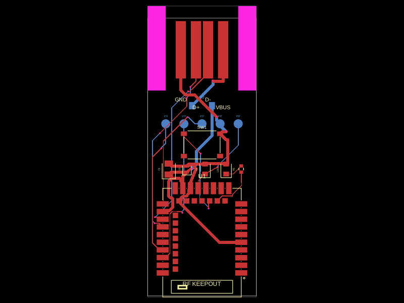
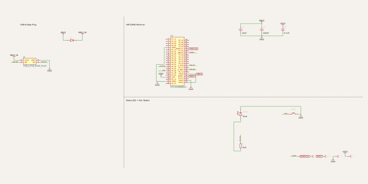
This code defines the physical layout and key components of a USB-C dongle featuring an nRF52840 microcontroller with antenna, USB-A connector, status LED, pair button, firmware debug test points, and associated passive components and interface connectors.
- Version
- 1.0.0
- License
- unset
- Stars
- 0
dongle.circuit.tsx
PCB
Schematic
import { Fragment } from "react"
import type { ConnectorProps } from "@tscircuit/props"
import { E73_2G4M08S1C } from "./imports/E73_2G4M08S1C"
import { TS_1187A_B_A_B } from "./imports/TS_1187A_B_A_B"
import { SS14L } from "./imports/SS14L"

/*
 * FALCHION-65 2.4 GHz DONGLE
 *
 * A second nRF52840 on a USB-A stick. It is the receiver half of the
 * low-latency link: the keyboard talks to it over Nordic's 2.4 GHz protocol
 * (or ZMK's BLE-based dongle mode) and the dongle presents itself to the PC
 * as a plain USB HID keyboard, so the host needs no driver and no Bluetooth.
 *
 * The nRF52840 runs straight from the USB 5 V through its VDDH pin -- REG0
 * makes the 3.3 V rail internally -- so the whole dongle is one module, four
 * passives, a button and an LED.
 *
 * Board: 18 x 46 mm, with a 12 mm wide tongue at the top formed by two edge
 * notches. The four gold fingers on the tongue ARE the USB-A plug.
 *
 * TONGUE GEOMETRY (verified against the Molex 67643 USB-A receptacle
 * footprint, whose pins sit at 0 / 2.5 / 4.5 / 7.0 mm): the four contacts
 * are NOT on a uniform pitch. VBUS and GND are 3.5 mm off centre, D- and D+
 * are 1.0 mm off centre. Fingers are 1.7 mm wide, so the gaps are 0.8 mm.
 *
 * ORIENTATION: with the dongle lying pads-up and the tongue pointing away
 * from you, VBUS is the RIGHT-hand finger and GND the left-hand one. D1, a
 * Schottky in series with VBUS, means a mirrored tongue simply does nothing
 * (the reverse path is blocked) instead of destroying the module, so if the
 * first board does not enumerate, measure the fingers with a meter: +5 V on
 * the finger marked VBUS relative to the one marked GND means correct, -5 V
 * means mirror the fingers in the next revision.
 *
 * Order the PCB 2.0 mm thick with gold fingers (ENIG + 45 deg bevel); a
 * 1.6 mm board fits loosely and needs tape on the back of the tongue.
 */

const BOARD = { width: 18, height: 46 }
const TONGUE = {
  width: 12,
  yStart: 11, // where the tongue begins
  yEnd: BOARD.height / 2, // 23, the leading edge
}
const FINGER = {
  // contact centre positions across the tongue, +x = right when pads are up
  // and the tongue points away: GND, D+, D-, VBUS
  x: { GND: -3.5, DP: -1.0, DM: 1.0, VBUS: 3.5 },
  width: 1.7,
  length: 9.5,
  yCenter: (TONGUE.yStart + TONGUE.yEnd) / 2 + 0.75,
}

/* The USB-A plug, as four gold fingers on the top copper of the tongue.
   Pin numbers follow the USB-A standard (1 VBUS, 2 D-, 3 D+, 4 GND). */
const USB_A_EDGE_PLUG = (props: ConnectorProps) => (
  <connector
    {...props}
    manufacturerPartNumber="USB_A_PCB_EDGE_PLUG"
    pinLabels={{
      pin1: ["VBUS"],
      pin2: ["DM"],
      pin3: ["DP"],
      pin4: ["GND"],
    }}
    footprint={
      <footprint>
        <smtpad
          portHints={["pin1"]}
          shape="rect"
          pcbX={`${FINGER.x.VBUS}mm`}
          pcbY="0mm"
          width={`${FINGER.width}mm`}
          height={`${FINGER.length}mm`}
        />
        <smtpad
          portHints={["pin2"]}
          shape="rect"
          pcbX={`${FINGER.x.DM}mm`}
          pcbY="0mm"
          width={`${FINGER.width}mm`}
          height={`${FINGER.length}mm`}
        />
        <smtpad
          portHints={["pin3"]}
          shape="rect"
          pcbX={`${FINGER.x.DP}mm`}
          pcbY="0mm"
          width={`${FINGER.width}mm`}
          height={`${FINGER.length}mm`}
        />
        <smtpad
          portHints={["pin4"]}
          shape="rect"
          pcbX={`${FINGER.x.GND}mm`}
          pcbY="0mm"
          width={`${FINGER.width}mm`}
          height={`${FINGER.length}mm`}
        />
      </footprint>
    }
  />
)

export default () => (
  <board width={`${BOARD.width}mm`} height={`${BOARD.height}mm`} thickness="2mm">
    <net name="GND" isGroundNet />
    <net name="VBUS" isPowerNet />
    <net name="V3V3" isPowerNet />

    <schematicsection name="Usb" displayName="USB-A Edge Plug" />
    <schematicsection name="Mcu" displayName="nRF52840 Receiver" />
    <schematicsection name="Io" displayName="Status LED + Pair Button" />

    {/* Two notches cut the 18 mm board down to a 12 mm tongue. Each runs
        1 mm past the leading edge so the corner comes out square. */}
    {[-1, 1].map((side) => (
      <Fragment key={`notch${side}`}>
        <cutout
          shape="rect"
          width="3.0mm"
          height={`${TONGUE.yEnd - TONGUE.yStart + 2}mm`}
          pcbX={`${side * (BOARD.width / 2 - 1.5)}mm`}
          pcbY={`${(TONGUE.yStart + TONGUE.yEnd) / 2 + 1}mm`}
        />
      </Fragment>
    ))}

    {/* ============================ USB-A plug ============================ */}
    <USB_A_EDGE_PLUG
      name="J1"
      pcbX={0}
      pcbY={FINGER.yCenter}
      schSectionName="Usb"
      schX={-14}
      schY={0}
    />
    <silkscreentext text="GND" pcbX={FINGER.x.GND} pcbY={TONGUE.yStart - 1.5} fontSize="0.9mm" />
    <silkscreentext text="D+" pcbX={FINGER.x.DP} pcbY={TONGUE.yStart - 2.8} fontSize="0.9mm" />
    <silkscreentext text="D-" pcbX={FINGER.x.DM} pcbY={TONGUE.yStart - 1.5} fontSize="0.9mm" />
    <silkscreentext text="VBUS" pcbX={FINGER.x.VBUS} pcbY={TONGUE.yStart - 2.8} fontSize="0.9mm" />
    <trace from="J1.VBUS" to="net.VBUS_IN" thickness="0.5mm" />
    {/* Reverse-insertion guard: blocks the path that a mirrored tongue would
        otherwise drive backwards through the module. ~0.3 V drop; VDDH is
        happy anywhere from 2.5 to 5.5 V. */}
    <SS14L name="D1" layer="bottom" pcbX={0} pcbY={8.5} schSectionName="Usb" schX={-10} schY={2} />
    <trace from="D1.anode" to="net.VBUS_IN" thickness="0.5mm" />
    <trace from="D1.cathode" to="net.VBUS" thickness="0.5mm" />
    <trace from="J1.GND" to="net.GND" thickness="0.5mm" />
    <trace from="J1.DP" to="net.USB_DP" />
    <trace from="J1.DM" to="net.USB_DM" />

    {/* ============================ nRF52840 ============================ */}
    {/* Antenna points at the far end of the stick, away from the USB shell
        and the host's metal chassis. VBUS drives VDDH; REG0 makes 3.3 V. */}
    <E73_2G4M08S1C
      name="U1"
      pcbX={0}
      pcbY={-13}
      schSectionName="Mcu"
      schX={0}
      schY={0}
      connections={{
        VDDH: "net.VBUS",
        VBUS: "net.VBUS",
        VDD: "net.V3V3",
        D_POS: "net.USB_DP",
        D_NEG: "net.USB_DM",
        RESET: "net.NRST",
        SWDIO: "net.SWDIO",
        SWDCLK: "net.SWDCLK",
        P0_06: "net.STATUS",
        P0_08: "net.PAIR",
        GND1: "net.GND",
        GND2: "net.GND",
        GND3: "net.GND",
      }}
    />
    <silkscreentext text="RF KEEPOUT" pcbX={0} pcbY={-21} fontSize="1mm" />
    <capacitor name="C1" capacitance="10uF" footprint="0805" pcbX={-5.5} pcbY={-2} pcbRotation={90} schSectionName="Mcu" schX={6} schY={3} schOrientation="vertical" />
    <capacitor name="C2" capacitance="100nF" footprint="0402" pcbX={-2.5} pcbY={-2} pcbRotation={90} schSectionName="Mcu" schX={8} schY={3} schOrientation="vertical" />
    <capacitor name="C3" capacitance="4.7uF" footprint="0603" pcbX={0.5} pcbY={-2} pcbRotation={90} schSectionName="Mcu" schX={10} schY={3} schOrientation="vertical" />
    <trace from="C1.pin1" to="net.VBUS" />
    <trace from="C1.pin2" to="net.GND" />
    <trace from="C2.pin1" to="net.VBUS" />
    <trace from="C2.pin2" to="net.GND" />
    <trace from="C3.pin1" to="net.V3V3" />
    <trace from="C3.pin2" to="net.GND" />

    {/* ============================ Status LED + pair button ============================ */}
    <led name="LED1" color="blue" footprint="0603" pcbX={4} pcbY={-2} pcbRotation={90} schSectionName="Io" schX={6} schY={-5} schRotation={90} />
    <resistor name="R1" resistance="1k" footprint="0402" pcbX={6.5} pcbY={-2} pcbRotation={90} schSectionName="Io" schX={6} schY={-8} schOrientation="vertical" />
    <trace from="net.STATUS" to="R1.pin1" />
    <trace from="R1.pin2" to="LED1.anode" />
    <trace from="LED1.cathode" to="net.GND" />
    <TS_1187A_B_A_B name="SW1" pcbX={0} pcbY={2} schSectionName="Io" schX={11} schY={-5} />
    <trace from="SW1.pin1" to="net.PAIR" />
    <trace from="SW1.pin2" to="net.GND" />

    {/* SWD + reset, for flashing the receiver firmware */}
    {[
      { name: "TP1", net: "net.SWDIO", x: -6 },
      { name: "TP2", net: "net.SWDCLK", x: -3 },
      { name: "TP3", net: "net.NRST", x: 0 },
      { name: "TP4", net: "net.GND", x: 3 },
      { name: "TP5", net: "net.V3V3", x: 6 },
    ].map((tp) => (
      <Fragment key={tp.name}>
        <testpoint
          name={tp.name}
          footprintVariant="pad"
          padShape="circle"
          padDiameter="1.5mm"
          layer="bottom"
          pcbX={tp.x}
          pcbY={5.5}
          schSectionName="Io"
          schX={14 + tp.x * 0.4}
          schY={-9}
        />
        <trace from={`${tp.name}.pin1`} to={tp.net} />
      </Fragment>
    ))}
  </board>
)