pixalynx/esp32-usb-ducky
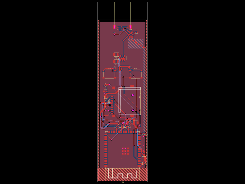
This design features a PCB with key components including an SOT-223 AMS1117 voltage regulator, a USB Type-C connector with ESD protection array, an ESP32-S3-WROOM-1 module with integrated USB, a microSD card socket, power management chips, status LED, reset and boot buttons, and associated decoupling and signal routing, all arranged on a compact 26mm x 84.5mm dual-layer PCB.
- Version
- 1.2.4
- License
- unset
- Stars
- 0
index.circuit.tsx
PCB
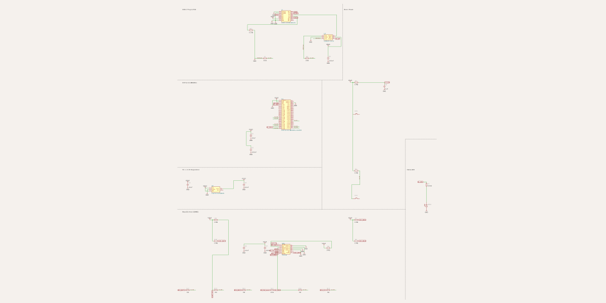
Schematic
import { ESP32_S3_WROOM_1_N16R8 } from "./imports/ESP32_S3_WROOM_1_N16R8"
import { TLV75733PDBVR } from "./imports/TLV75733PDBVR"
import { USBLC6_2SC6 } from "./imports/USBLC6_2SC6"
import { TF_01A } from "./imports/TF_01A"
import { TS_1187A_B_A_B } from "./imports/TS_1187A_B_A_B"
import { U261_121N_4BS2S } from "./imports/U261_121N_4BS2S"
import { XL_1608UBC_04 } from "./imports/XL_1608UBC_04"

// Schematic sections on a compact grid.
const SEC = {
  Usb: { x: 0, y: 16 },
  Mcu: { x: 0, y: 2 },
  BootReset: { x: 10, y: 2 },
  Power: { x: -10, y: -8 },
  Indicator: { x: 20, y: -8 },
  MicroSd: { x: 0, y: -20 },
}

// Board outline is a plain 26 x 84.5mm stick. The USB-C male plug (J1) is a
// board-edge part: only its 4.65mm rear flange sits on the PCB and the ~9mm
// plug body overhangs the TOP edge (y = +35.5) to insert straight into a host.
// Per the XKB datasheet's recommended layout the PCB edge is 4.65mm ahead of
// the connector's rear face, i.e. ~4.0mm ahead of the signal-pad centres —
// with J1 at pcbY=32 (pads at y=31.5) the 35.5 edge lands on that line.
// The ESP32 module lives at the BOTTOM with its printed antenna right at the
// bottom edge, as far from the USB metal as the board allows.
//   top edge (USB-C plug)   y = +35.5
//   bottom edge (antenna)   y = -49
const BOARD_OUTLINE = [
  { x: -13, y: -49 },
  { x: 13, y: -49 },
  { x: 13, y: 35.5 },
  { x: -13, y: 35.5 },
]

// U1 is placed antenna-down (pcbRotation=180) at the bottom. Its printed
// antenna (the module's own meander) now sits flush at the bottom board edge
// with no copper around or under it — the proper spot for RF, well clear of
// the USB shell up top. The keepout spans the FULL board width (26mm) so the
// GND pours can't fill the strips beside the antenna down to the board edge
// (Espressif's module guidelines want the sides of the antenna clear, not just
// the area under it).
const ANTENNA_KEEPOUT = { pcbX: 0, pcbY: -45.65, width: 26.2, height: 6.6 }

export default () => (
  <board
    width="26mm"
    height="84.5mm"
    layers={2}
    thickness="1.6mm"
    outline={BOARD_OUTLINE}
    title="ESP32-S3 USB-C Stick"
    // Autorouter vias: 0.3mm hole / 0.5mm pad = 0.1mm annular ring, the
    // minimum JLCPCB accepts (they prefer 0.15mm; bump the pad to 0.6mm if
    // routing density allows).
    pcbStyle={{ viaHoleDiameter: "0.3mm", viaPadDiameter: "0.5mm" }}
  >
    <net name="GND" isGroundNet />
    <net name="VBUS" isPowerNet />
    <net name="V3V3" isPowerNet />

    <schematicsection name="Usb" displayName="USB-C Plug & ESD" />
    <schematicsection name="Mcu" displayName="ESP32-S3-WROOM-1" />
    <schematicsection name="BootReset" displayName="Boot / Reset" />
    <schematicsection name="Power" displayName="5V -> 3.3V Regulation" />
    <schematicsection name="Indicator" displayName="Status LED" />
    <schematicsection name="MicroSd" displayName="MicroSD (4-bit SDMMC)" />

    {/* ===================== USB-C male plug (C2879827) ===================== */}
    {/* XKB U261-121N-4BS2S: a solder-on, right-angle, surface-mount USB-C MALE
        plug. It mounts flat on the board and the plug overhangs the top edge to
        insert straight into a host. USB 2.0 device wiring: VBUS/GND on their
        pins, one CC line with a 5.1k Rd to GND (correct for a plug), and D+/D-
        through the ESD array + 22ohm resistors. SuperSpeed pins are unused. */}
    <U261_121N_4BS2S
      name="J1"
      pcbX={0}
      pcbY={32}
      pcbRotation={180}
      schX={SEC.Usb.x}
      schY={SEC.Usb.y}
      schSectionName="Usb"
    />

    {/* CC pull-down (5.1k Rd) presents the board as a USB device (sink) */}
    <resistor name="R11" resistance="5.1k" footprint="0402" pcbX={-4} pcbY={28.5}
      schSectionName="Usb" schX={SEC.Usb.x - 5} schY={SEC.Usb.y - 2} />

    {/* Low-capacitance ESD array 2.7mm behind the plug's D+/D- pads (A6/A7 at
        y=31.5; U3's top pin row is at y=28.95). Flow-through: the plug feeds
        the TOP row (IO1_B pin6 / IO2_B pin4), the chip clamps, and the BOTTOM
        row (IO1 pin1 / IO2 pin3) carries the pair on to the MCU — the two
        pins of each channel are bonded inside the USBLC6, so either works. */}
    <USBLC6_2SC6
      name="U3"
      pcbX={4.5}
      pcbY={27.8}
      schSectionName="Usb"
      schX={SEC.Usb.x + 6}
      schY={SEC.Usb.y - 3}
    />

    {/* USB series resistors on D+/D- between the ESD array and the MCU. They
        sit side by side at the bottom of the hand-routed D+/D- lane (x=11.4 /
        11.8) with pin1 facing up into the lane and pin2 facing U1.IO20/IO19
        at (8.75,-24.5)/(8.75,-25.8). */}
    <resistor
      name="R3"
      resistance="22"
      footprint="0402"
      pcbX={10.85}
      pcbY={-24.5}
      pcbRotation={270}
      schSectionName="Usb"
      schX={SEC.Usb.x + 3}
      schY={SEC.Usb.y - 6}
    />
    <resistor
      name="R4"
      resistance="22"
      footprint="0402"
      pcbX={11.85}
      pcbY={-24.5}
      pcbRotation={270}
      schSectionName="Usb"
      schX={SEC.Usb.x - 3}
      schY={SEC.Usb.y - 6}
    />

    {/* VBUS + GND (both VBUS pins, all GND pins + shell tabs) */}
    <trace from="J1.VBUS1" to="net.VBUS" thickness="0.4mm" />
    <trace from="J1.VBUS2" to="net.VBUS" thickness="0.4mm" />
    <trace from="J1.GND1" to="net.GND" />
    <trace from="J1.GND2" to="net.GND" />
    <trace from="J1.GND3" to="net.GND" />
    <trace from="J1.SHELL1" to="net.GND" />
    <trace from="J1.SHELL2" to="net.GND" />
    {/* single CC line -> 5.1k Rd -> GND */}
    <trace from="J1.CC1" to="R11.pin1" />
    <trace from="R11.pin2" to="net.GND" />
    {/* Data -> ESD -> 22ohm series -> ESP32. D+ uses the USBLC6's IO1
        channel, D- its IO2 channel. */}
    <trace from="J1.DP1" to="U3.IO1_B" />
    <trace from="J1.DN1" to="U3.IO2_B" />
    <trace from="U3.GND" to="net.GND" />
    <trace from="U3.VBUS" to="net.VBUS" />
    {/* Hand-routed D+/D- pair (top layer, 0.2mm wide, 0.4mm centre spacing): straight
        down out of U3's bottom pins, one parallel diagonal to the right-edge
        lane at x=11.4/11.8, then a 44mm straight run to R3/R4. pcbPath points
        are offsets from U3's centre (4.5, 27.8); the `to` pad is appended
        automatically. The lane is shadowed by top-layer keepouts (below) so
        the autorouter can't cross it — it does not treat manual copper as an
        obstacle on its own. */}
    <trace
      name="USB_DP_pair"
      from="U3.IO1"
      to="R3.pin1"
      thickness="0.2mm"
      pcbPath={[
        { x: -0.95, y: -2.2 },
        { x: 6.9, y: -7.0 },
        { x: 6.9, y: -50.8 },
        { x: 6.35, y: -51.35 },
      ]}
    />
    <trace
      name="USB_DN_pair"
      from="U3.IO2"
      to="R4.pin1"
      thickness="0.2mm"
      pcbPath={[
        { x: 0.95, y: -2.893 },
        { x: 7.3, y: -6.776 },
        { x: 7.3, y: -50.8 },
        { x: 7.35, y: -51.35 },
      ]}
    />
    {/* ST-recommended 100nF right on the USBLC6 VBUS pin (GPT review #5) */}
    <capacitor name="C9" capacitance="100nF" footprint="0402" pcbX={7.5} pcbY={29}
      schOrientation="vertical"
      schSectionName="Usb" schX={SEC.Usb.x + 6} schY={SEC.Usb.y - 6} />
    <trace from="C9.pin1" to="net.VBUS" />
    <trace from="C9.pin2" to="net.GND" />

    {/* ===================== 5V -> 3.3V regulation ===================== */}
    {/* TLV75733 (1A LDO) — ceramic-cap stable, so the ceramic input/output caps
        are now within spec (the AMS1117 wanted tantalum). 1A gives headroom for
        WiFi TX bursts + microSD. EN is tied to VIN so the LDO is always on. */}
    <TLV75733PDBVR
      name="U2"
      pcbX={0}
      pcbY={15.5}
      schSectionName="Power"
      schX={SEC.Power.x}
      schY={SEC.Power.y - 0.68}
    />
    {/* C1 (VBUS in) sits 1.7mm from U2.IN (pin1, bottom-left) and C2 (V3V3
        out) 1.7mm from U2.OUT (pin5, top-left); both are rotated so the rail
        pad faces the LDO pin and the GND pad faces outward. */}
    <capacitor
      name="C1"
      capacitance="10uF"
      footprint="0805"
      schOrientation="vertical"
      pcbX={-3.5}
      pcbY={13.6}
      pcbRotation={180}
      schSectionName="Power"
      schX={SEC.Power.x - 4}
      schY={SEC.Power.y}
    />
    <capacitor
      name="C2"
      capacitance="22uF"
      footprint="0805"
      supplierPartNumbers={{ jlcpcb: ["C45783"] }}
      schOrientation="vertical"
      pcbX={-3.5}
      pcbY={17.4}
      pcbRotation={180}
      schSectionName="Power"
      schX={SEC.Power.x + 4}
      schY={SEC.Power.y}
    />
    <trace from="net.VBUS" to="U2.IN" thickness="0.4mm" />
    <trace from="U2.EN" to="net.VBUS" />
    <trace from="U2.GND" to="net.GND" />
    <trace from="U2.OUT" to="net.V3V3" thickness="0.8mm" />
    <trace from="C1.pin1" to="net.VBUS" thickness="0.4mm" />
    <trace from="C1.pin2" to="net.GND" />
    <trace from="C2.pin1" to="net.V3V3" thickness="0.4mm" />
    <trace from="C2.pin2" to="net.GND" />

    {/* ===================== Boot / Reset ===================== */}
    {/* EN: pull-up + power-on delay cap + reset button. */}
    <resistor
      name="R1"
      resistance="10k"
      footprint="0402"
      pcbX={-1}
      pcbY={10}
      schSectionName="BootReset"
      schX={SEC.BootReset.x}
      schY={SEC.BootReset.y + 4.58}
    />
    <capacitor
      name="C5"
      capacitance="1uF"
      footprint="0402"
      schOrientation="vertical"
      pcbX={-4}
      pcbY={10}
      schSectionName="BootReset"
      schX={SEC.BootReset.x + 4}
      schY={SEC.BootReset.y + 4}
    />
    <TS_1187A_B_A_B
      name="SW2"
      pcbX={-7}
      pcbY={7}
      schSectionName="BootReset"
      schX={SEC.BootReset.x}
      schY={SEC.BootReset.y}
    />
    <trace from="U1.EN" to="R1.pin2" />
    <trace from="U1.EN" to="C5.pin1" />
    <trace from="U1.EN" to="SW2.pin1" />
    <trace from="R1.pin1" to="net.V3V3" />
    <trace from="C5.pin2" to="net.GND" />
    {/* TS-1187A internal wiring (XKB datasheet): A(pin1)-B(pin2) are one
        terminal, C(pin3)-D(pin4) the other; A/B is the TOP row and C/D the
        BOTTOM row of the footprint. The switch closes A/B <-> C/D, so the
        signal goes to the top row and GND to the bottom row. (Tying pin1 to
        pin3 as before shorted EN straight to GND through the A-B bond.) */}
    <trace from="SW2.pin3" to="net.GND" />
    {/* tie each terminal's two redundant pads together */}
    <trace from="SW2.pin2" to="SW2.pin1" />
    <trace from="SW2.pin4" to="SW2.pin3" />

    {/* IO0/BOOT: pull-up + button to force the ROM download-mode bootloader. */}
    <resistor
      name="R2"
      resistance="10k"
      footprint="0402"
      pcbX={4}
      pcbY={10}
      schSectionName="BootReset"
      schX={SEC.BootReset.x}
      schY={SEC.BootReset.y - 8}
    />
    <TS_1187A_B_A_B
      name="SW1"
      pcbX={7}
      pcbY={7}
      schSectionName="BootReset"
      schX={SEC.BootReset.x}
      schY={SEC.BootReset.y - 12}
    />
    <trace from="U1.BOOT" to="R2.pin2" />
    <trace from="U1.BOOT" to="SW1.pin1" />
    <trace from="R2.pin1" to="net.V3V3" />
    {/* same A/B-top, C/D-bottom terminal pairing as SW2 */}
    <trace from="SW1.pin3" to="net.GND" />
    <trace from="SW1.pin2" to="SW1.pin1" />
    <trace from="SW1.pin4" to="SW1.pin3" />

    {/* ===================== Status LED ===================== */}
    <resistor
      name="R5"
      resistance="330"
      footprint="0402"
      schOrientation="vertical"
      pcbX={-9}
      pcbY={1}
      schSectionName="Indicator"
      schX={SEC.Indicator.x}
      schY={SEC.Indicator.y}
    />
    {/* XL-1608UBC-04 blue LED (C965807): pin1 is CATHODE, pin2 is ANODE, so
        wire by the named anode/cathode ports to guarantee correct polarity. */}
    <XL_1608UBC_04
      name="LED1"
      schRotation={90}
      pcbX={-9}
      pcbY={-2}
      schSectionName="Indicator"
      schX={SEC.Indicator.x}
      schY={SEC.Indicator.y - 3}
    />
    <trace from="U1.LED_GPIO" to="R5.pin1" />
    <trace from="R5.pin2" to="LED1.anode" />
    <trace from="LED1.cathode" to="net.GND" />

    {/* ===================== MicroSD (4-bit SDMMC) ===================== */}
    {/* Native SDMMC host, 4-bit bus, via the S3 GPIO matrix:
          CLK = GPIO12 (22R R13)   CMD = GPIO11   D0 = GPIO13
          D1  = GPIO14             D2  = GPIO21   D3 = GPIO10
        The TF-01A import keeps its SPI-era pin aliases; physically
        SD1.CS = DAT3, SD1.MOSI = CMD, SD1.SCK = CLK, SD1.MISO = DAT0, and
        SD1.DAT1/DAT2 are DAT1/DAT2. Socket placement unchanged: middle of
        the board (card inserts from the side edge), well away from the
        antenna at the bottom. */}
    <TF_01A
      name="SD1"
      pcbX={0}
      pcbY={-7}
      pcbRotation={90}
      schHeight={1.4}
      schSectionName="MicroSd"
      schX={SEC.MicroSd.x}
      schY={SEC.MicroSd.y + 2.82}
    />
    <resistor
      name="R6"
      resistance="10k"
      footprint="0402"
      pcbX={4.5}
      pcbY={-16.6}
      schSectionName="MicroSd"
      schX={SEC.MicroSd.x + 6}
      schY={SEC.MicroSd.y + 3}
    />
    {/* Dedicated decoupling at the card's own supply pins. */}
    <capacitor
      name="C7"
      capacitance="100nF"
      footprint="0402"
      schOrientation="vertical"
      pcbX={-8.5}
      pcbY={-5}
      schSectionName="MicroSd"
      schX={SEC.MicroSd.x - 3}
      schY={SEC.MicroSd.y + 3}
    />
    <capacitor
      name="C8"
      capacitance="10uF"
      footprint="0805"
      schOrientation="vertical"
      pcbX={7}
      pcbY={-18.5}
      schSectionName="MicroSd"
      schX={SEC.MicroSd.x - 6}
      schY={SEC.MicroSd.y + 3}
    />
    {/* SDMMC pull-ups (10k to 3V3, one per line, on the card side of the
        series resistors): R6 = DAT3, R7 = CMD, R8 = DAT0, R9 = DAT1,
        R10 = DAT2. CLK is push-pull driven and has NO pull-up. */}
    <resistor
      name="R7"
      resistance="10k"
      footprint="0402"
      pcbX={3.5}
      pcbY={-18.5}
      schSectionName="MicroSd"
      schX={SEC.MicroSd.x + 10}
      schY={SEC.MicroSd.y + 7}
    />
    <resistor
      name="R8"
      resistance="10k"
      footprint="0402"
      pcbX={-2}
      pcbY={-19}
      schSectionName="MicroSd"
      schX={SEC.MicroSd.x + 10}
      schY={SEC.MicroSd.y + 4}
    />
    <resistor
      name="R9"
      resistance="10k"
      footprint="0402"
      pcbX={-9}
      pcbY={-8}
      schSectionName="MicroSd"
      schX={SEC.MicroSd.x - 10}
      schY={SEC.MicroSd.y + 7}
    />
    <resistor
      name="R10"
      resistance="10k"
      footprint="0402"
      pcbX={-9}
      pcbY={-11}
      schSectionName="MicroSd"
      schX={SEC.MicroSd.x - 10}
      schY={SEC.MicroSd.y + 4}
    />
    <trace from="SD1.VDD" to="net.V3V3" thickness="0.4mm" />
    <trace from="C7.pin1" to="net.V3V3" />
    <trace from="C8.pin1" to="net.V3V3" thickness="0.4mm" />
    <trace from="SD1.VSS" to="net.GND" />
    <trace from="C7.pin2" to="net.GND" />
    <trace from="C8.pin2" to="net.GND" />
    <trace from="SD1.GND1" to="net.GND" />
    <trace from="SD1.GND2" to="net.GND" />
    <trace from="SD1.GND3" to="net.GND" />
    <trace from="SD1.GND4" to="net.GND" />
    {/* Series resistors, one per SDMMC line, in a row 2mm above the module's
        pin row with each resistor directly over its GPIO pad (pitch 1.27mm
        = the module's pin pitch), rotated 270 so pin1 faces the card and pin2
        faces the MCU (rotation 90 puts them the other way round).
        R13 keeps its 22R on CLK (Espressif SD guidance); the other five are
        0R placeholders that give 40MHz tuning options without a re-spin. */}
    <resistor name="R14" resistance="0" footprint="0402" pcbX={3.18} pcbY={-20.8} pcbRotation={270}
      schSectionName="MicroSd" schX={SEC.MicroSd.x + 6} schY={SEC.MicroSd.y - 3} />
    <resistor name="R15" resistance="0" footprint="0402" pcbX={1.91} pcbY={-20.8} pcbRotation={270}
      schSectionName="MicroSd" schX={SEC.MicroSd.x + 2} schY={SEC.MicroSd.y - 3} />
    <resistor
      name="R13"
      resistance="22"
      footprint="0402"
      pcbX={0.64}
      pcbY={-20.8}
      pcbRotation={270}
      schSectionName="MicroSd"
      schX={SEC.MicroSd.x - 2}
      schY={SEC.MicroSd.y - 3}
    />
    <resistor name="R16" resistance="0" footprint="0402" pcbX={-0.63} pcbY={-20.8} pcbRotation={270}
      schSectionName="MicroSd" schX={SEC.MicroSd.x - 6} schY={SEC.MicroSd.y - 3} />
    <resistor name="R17" resistance="0" footprint="0402" pcbX={-1.9} pcbY={-20.8} pcbRotation={270}
      schSectionName="MicroSd" schX={SEC.MicroSd.x - 10} schY={SEC.MicroSd.y - 3} />
    <resistor name="R18" resistance="0" footprint="0402" pcbX={-3.17} pcbY={-20.8} pcbRotation={270}
      schSectionName="MicroSd" schX={SEC.MicroSd.x - 14} schY={SEC.MicroSd.y - 3} />

    {/* DAT3: SD1.CS pad -> R14 -> GPIO10, pulled up by R6 */}
    <trace from="SD1.CS" to="R14.pin1" />
    <trace from="R14.pin2" to="U1.SD_D3" />
    <trace from="SD1.CS" to="R6.pin2" />
    <trace from="R6.pin1" to="net.V3V3" />
    {/* CMD: SD1.MOSI pad -> R15 -> GPIO11, pulled up by R7 */}
    <trace from="SD1.MOSI" to="R15.pin1" />
    <trace from="R15.pin2" to="U1.SD_CMD" />
    <trace from="R7.pin1" to="net.V3V3" />
    <trace from="R7.pin2" to="SD1.MOSI" />
    {/* CLK: SD1.SCK pad -> R13 (22R) -> GPIO12, no pull-up. Hand-routed
        (0.2mm, ~26mm, two vias): 1.1mm out of the pad on top, via to the
        bottom layer, west to x=-10.6 (past the R9/R10 pull-ups), straight
        down past the socket, one shallow diagonal to x=0.64, via back up 2mm
        above R13 and straight into it. The bottom-layer detour is
        deliberate: a CLK wall on either layer next to the pad column starved
        the autorouter of exits/vias for the other five lines (it ran out of
        iterations, then dropped vias onto pads); out at x=-10.6 nothing else
        needs that copper, and CMD/D0-D3 stay planar on top. pcbPath points are
        offsets in SD1's local frame (centre (0,-7), rotated 90:
        local = (by+7, -bx)); shadowed by the SD CLK keepouts below. */}
    <trace
      name="SD_CLK_lane"
      from="SD1.SCK"
      to="R13.pin1"
      thickness="0.2mm"
      pcbPath={[
        { x: -2.16, y: 6.6 },
        { x: -2.16, y: 6.6, via: true, toLayer: "bottom" },
        { x: -2.16, y: 6.6 },
        { x: -2.16, y: 10.6 },
        { x: -9.6, y: 10.6 },
        { x: -11.3, y: -0.64 },
        { x: -11.3, y: -0.64, via: true, toLayer: "top" },
        { x: -11.3, y: -0.64 },
      ]}
    />
    <trace from="R13.pin2" to="U1.SD_CLK" />
    {/* DAT0: SD1.MISO pad -> R16 -> GPIO13, pulled up by R8 */}
    <trace from="SD1.MISO" to="R16.pin1" />
    <trace from="R16.pin2" to="U1.SD_D0" />
    <trace from="R8.pin1" to="net.V3V3" />
    <trace from="R8.pin2" to="SD1.MISO" />
    {/* DAT1: SD1.DAT1 pad -> R17 -> GPIO14, pulled up by R9 */}
    <trace from="SD1.DAT1" to="R17.pin1" />
    <trace from="R17.pin2" to="U1.SD_D1" />
    <trace from="R9.pin1" to="net.V3V3" />
    <trace from="R9.pin2" to="SD1.DAT1" />
    {/* DAT2: SD1.DAT2 pad -> R18 -> GPIO21, pulled up by R10 */}
    <trace from="SD1.DAT2" to="R18.pin1" />
    <trace from="R18.pin2" to="U1.SD_D2" />
    <trace from="R10.pin1" to="net.V3V3" />
    <trace from="R10.pin2" to="SD1.DAT2" />

    {/* ===================== MCU (bottom, antenna at edge) ===================== */}
    <ESP32_S3_WROOM_1_N16R8
      name="U1"
      pcbX={0}
      pcbY={-32}
      pcbRotation={180}
      schHeight={4.2}
      schSectionName="Mcu"
      schX={SEC.Mcu.x}
      schY={SEC.Mcu.y}
    />

    <trace from="R4.pin2" to="U1.USB_D_NEG" />
    <trace from="R3.pin2" to="U1.USB_D_POS" />

    {/* Espressif's recommended land pattern stitches the module's centre GND
        pad to the bottom plane with a 3x3 via array. Those vias live inside
        the footprint (imports/ESP32_S3_WROOM_1_N16R8.tsx) as plated holes
        co-located with the nine pin41 paste pads, because free-standing
        <via>s overlapping the pads make the autorouter abort. */}
    <trace from="U1.3V3" to="net.V3V3" thickness="0.4mm" />
    <trace from="U1.GND1" to="net.GND" />
    <trace from="U1.GND2" to="net.GND" />
    {/* U1.GND3 (centre pad) is internally bonded to GND1/GND2 (see import);
        the GND pour and its 3x3 via-in-pad array tie it to both planes. */}

    {/* MCU decoupling in the strip beside the module's 3V3 pad (right edge,
        y=-39.8): C4 (100nF) right at the pin, C3 (10uF bulk) just above it. */}
    <capacitor
      name="C3"
      capacitance="10uF"
      footprint="0805"
      schOrientation="vertical"
      pcbX={11.3}
      pcbY={-34.5}
      pcbRotation={90}
      schSectionName="Mcu"
      schX={SEC.Mcu.x - 5}
      schY={SEC.Mcu.y - 3}
    />
    <capacitor
      name="C4"
      capacitance="100nF"
      footprint="0402"
      schOrientation="vertical"
      pcbX={11.3}
      pcbY={-39.5}
      pcbRotation={90}
      schSectionName="Mcu"
      schX={SEC.Mcu.x - 5}
      schY={SEC.Mcu.y - 5}
    />
    <trace from="C3.pin1" to="net.V3V3" thickness="0.4mm" />
    <trace from="C3.pin2" to="net.GND" />
    <trace from="C4.pin1" to="net.V3V3" />
    <trace from="C4.pin2" to="net.GND" />

    {/* Edge fences: 0.8mm routing keepouts along both long edges (x 12.2..13
        and -13..-12.2) so the autorouter can never hug the board edge — it
        otherwise pushes traces to x=12.7, inside the 0.275mm edge clearance
        (the USB D+/D- pair ended up there squeezing past R7/R8). */}
    <keepout shape="rect" layer="top" pcbX={12.7} pcbY={-6.75} width={0.6} height={84.5} />
    <keepout shape="rect" layer="bottom" pcbX={12.7} pcbY={-6.75} width={0.6} height={84.5} />

    {/* USB D+/D- lane fences (top layer only; the bottom pour stays as the
        pair's ground reference). KA/KB shadow the diagonal from U3's bottom
        pins to the lane, KL the straight lane itself down to just above
        R3/R4. Every rect keeps >0.1mm from neighbouring pads (U3 pads end at
        y=26.11, R6 at x=10.78, R3/R4 start at y=-23.72). */}
    {/* excludeRefs lets the DRC ignore the hand-routed pair (traces attached
        to U3/R3/R4) lying inside its own shadow keepouts; the autorouter
        still treats the rects as walls for everything else. */}
    <keepout shape="rect" layer="top" pcbX={7} pcbY={22.95} width={8} height={4.9} excludeRefs={[".U3", ".R3", ".R4"]} />
    <keepout shape="rect" layer="top" pcbX={4.6} pcbY={25.7} width={3.2} height={0.6} excludeRefs={[".U3", ".R3", ".R4"]} />
    <keepout shape="rect" layer="top" pcbX={11.7} pcbY={-1} width={1.4} height={45} excludeRefs={[".U3", ".R3", ".R4"]} />

    {/* SDMMC CLK lane shadows. The two manual vias are NOT shadowed (placement
        DRC treats via copper inside a keepout as an error and excludeRefs
        only covers components), so the rects stop >=0.1mm short of each via.
        BOTTOM layer: west run at y=-9.16, vertical at x=-10.6, chain of small
        rects along the shallow diagonal (-10.6,-16.6) -> (0.64,-18.3).
        TOP layer: the drop into R13. */}
    <keepout shape="rect" layer="bottom" pcbX={-8.9} pcbY={-9.16} width={3.9} height={0.5} excludeRefs={[".SD1", ".R13"]} />
    <keepout shape="rect" layer="bottom" pcbX={-10.6} pcbY={-12.88} width={0.5} height={7.9} excludeRefs={[".SD1", ".R13"]} />
    {Array.from({ length: 12 }, (_, i) => {
      const t = 0.03 + (i * (0.9244 - 0.03)) / 11
      const x = -10.6 + t * (0.64 + 10.6)
      const y = -16.6 + t * (-18.3 + 16.6)
      return (
        <keepout
          key={`sdclk_diag_${i}`}
          shape="rect"
          layer="bottom"
          pcbX={x}
          pcbY={y}
          width={1.0}
          height={0.5}
          excludeRefs={[".SD1", ".R13"]}
        />
      )
    })}
    <keepout shape="rect" layer="top" pcbX={0.64} pcbY={-19.25} width={0.4} height={1.3} excludeRefs={[".SD1", ".R13"]} />
    <keepout shape="rect" layer="top" pcbX={-12.6} pcbY={-6.75} width={0.8} height={84.5} />
    <keepout shape="rect" layer="bottom" pcbX={-12.6} pcbY={-6.75} width={0.8} height={84.5} />

    {/* Antenna keepout — no copper (traces, vias, or pour) around the module's
        printed antenna at the bottom edge. */}
    <keepout shape="rect" layer="top" {...ANTENNA_KEEPOUT} />
    <keepout shape="rect" layer="bottom" {...ANTENNA_KEEPOUT} />

    {/* Ground pour on both layers; pulled back from the board edge so it never
        reaches the tongue-tip contact area. */}
    {/* LDO heat-spreading: a bounded V3V3 pour joining U2.OUT (pin5 at
        x=-0.9,y=16.6) to C2's V3V3 pad, giving the regulator's output lead
        real copper area. Kept above y=15.6 so it stays clear of the IN/GND/EN
        pin row at y=14.4 (the old outline covered that row and the clearance
        rules ate the pour down to a 1.4mm blob). */}
    <copperpour
      name="U2_out_pour"
      connectsTo="net.V3V3"
      layer="top"
      outline={[
        { x: -6, y: 15.6 },
        { x: -0.2, y: 15.6 },
        { x: -0.2, y: 19 },
        { x: -6, y: 19 },
      ]}
    />
    <copperpour connectsTo="net.GND" layer="top" clearance="0.2mm" boardEdgeMargin="1mm" />
    <copperpour connectsTo="net.GND" layer="bottom" clearance="0.2mm" boardEdgeMargin="1mm" />
  </board>
)