olivergrabinski/tscircuit-weather
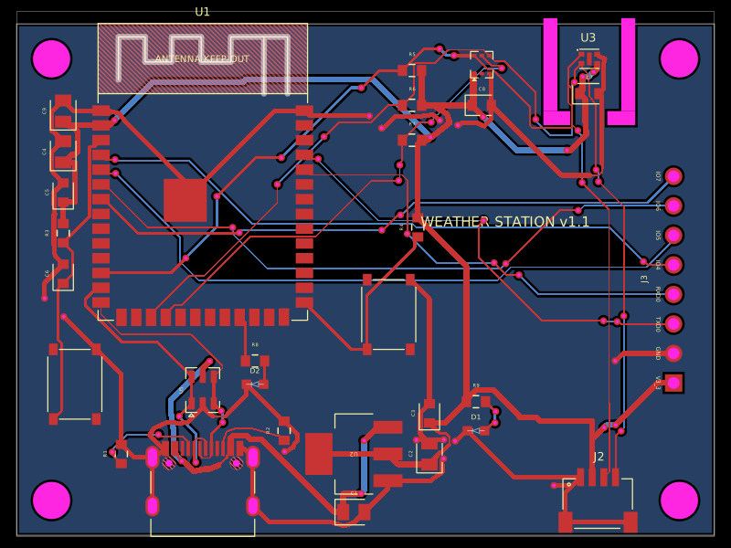
A 60×44 mm ESP32-S3 Wi‑Fi/BLE weather-station PCB with USB‑C power, 3.3 V regulation and ESD protection, temperature/humidity and UV/light sensors, status LEDs, buttons, Qwiic I²C expansion, debug GPIO header, and a printable enclosure.
- Version
- 1.2.0
- License
- unset
- Stars
- 0
index.circuit.tsx
PCB
Schematic

import { ESP32_S3_WROOM_1_N8R2 } from "./imports/ESP32_S3_WROOM_1_N8R2"
import { SHT40_AD1B_R3 } from "./imports/SHT40_AD1B_R3"
import { LTR_390UV_01 } from "./imports/LTR_390UV_01"
import { AMS1117_3_3 } from "./imports/AMS1117_3_3"
import { USBLC6_2SC6 } from "./imports/USBLC6_2SC6"
import { TS_1187A_B_A_B } from "./imports/TS_1187A_B_A_B"
import { KT_0603G } from "./imports/KT_0603G"
import { KT_0603B } from "./imports/KT_0603B"
import { JST_SH_SM04B_SRSS_TB } from "./imports/JST_SH_SM04B_SRSS_TB"
import { assembly, enclosure } from "tscircuit"

/**
 * Wi-Fi weather station
 *
 *  - ESP32-S3-WROOM-1 module: Wi-Fi + BLE, native USB (no UART bridge needed)
 *  - SHT40-AD1B: temperature + relative humidity, I2C 0x44
 *  - LTR-390UV-01: UV index + ambient light, I2C 0x53, INT on IO10
 *  - USB-C power/programming, AMS1117-3.3 LDO, USBLC6-2SC6 ESD protection
 *  - Qwiic (JST-SH 1.0 mm) I2C expansion + 8-pin debug/GPIO header
 *
 * Rev 1.1 (2026-09-24)
 *  - SHT40 sits on a thermal-isolation island: three 1.2 mm milled slots
 *    leave a 3.2 mm bridge at the bottom for the four traces, so heat from the
 *    LDO/module reaches the sensor only through that bridge.
 *  - <enclosure.fdm.box> models a printable case: window above the UV sensor,
 *    vent above the SHT40 island, holes for USB-C, Qwiic and both buttons.
 *
 * Fab rules: 0.25 mm signal traces (0.15 mm min), 0.5 mm 3V3/VBUS and 0.4 mm
 * GND traces, vias 0.3 mm drill / 0.6 mm pad,
 * i.e. within JLCPCB's standard 2-layer capability.
 *
 * ESP32-S3 pin plan
 *  IO8  SDA        IO9  SCL        IO10 UV_INT
 *  IO19 USB D-     IO20 USB D+     IO21 status LED
 *  IO0  BOOT       EN   RESET      IO4..IO7 spare ADC-capable GPIO on header
 *  TXD0/RXD0 UART0 on header
 */
/**
 * USB-C receptacle land pattern for HRO TYPE-C-31-M-12 (JLCPCB C165948),
 * copied from the exact EasyEDA footprint with its original pin numbering
 * (1-4 shell anchors, 5-12 signals, 13/14 GND, 15/16 VBUS) so the pick-and-
 * place rotation can be verified against the supplier part and the 3D model
 * lines up. Each shell anchor is its own pin, so every pad resolves to
 * exactly one port. The cable enters from -Y in this unrotated frame.
 */
const UsbC16Footprint = (
  <footprint insertionDirection="from_bottom">
    <platedhole portHints={["pin1"]} shape="pill" pcbX={4.325} pcbY={1.405} outerWidth={1.2} outerHeight={2.0} holeWidth={0.8} holeHeight={1.6} />
    <platedhole portHints={["pin2"]} shape="pill" pcbX={4.325} pcbY={-2.774} outerWidth={1.2} outerHeight={1.8} holeWidth={0.8} holeHeight={1.4} />
    <platedhole portHints={["pin3"]} shape="pill" pcbX={-4.325} pcbY={-2.774} outerWidth={1.2} outerHeight={1.8} holeWidth={0.8} holeHeight={1.4} />
    <platedhole portHints={["pin4"]} shape="pill" pcbX={-4.325} pcbY={1.405} outerWidth={1.2} outerHeight={2.0} holeWidth={0.8} holeHeight={1.6} />
    <smtpad portHints={["pin5"]} shape="rect" pcbX={-1.75} pcbY={2.174} width={0.3} height={1.3} />
    <smtpad portHints={["pin6"]} shape="rect" pcbX={-1.25} pcbY={2.174} width={0.3} height={1.3} />
    <smtpad portHints={["pin7"]} shape="rect" pcbX={-0.75} pcbY={2.174} width={0.3} height={1.3} />
    <smtpad portHints={["pin8"]} shape="rect" pcbX={-0.25} pcbY={2.174} width={0.3} height={1.3} />
    <smtpad portHints={["pin9"]} shape="rect" pcbX={0.25} pcbY={2.174} width={0.3} height={1.3} />
    <smtpad portHints={["pin10"]} shape="rect" pcbX={0.75} pcbY={2.174} width={0.3} height={1.3} />
    <smtpad portHints={["pin11"]} shape="rect" pcbX={1.25} pcbY={2.174} width={0.3} height={1.3} />
    <smtpad portHints={["pin12"]} shape="rect" pcbX={1.75} pcbY={2.174} width={0.3} height={1.3} />
    <smtpad portHints={["pin13"]} shape="rect" pcbX={-3.2} pcbY={2.174} width={0.6} height={1.3} />
    <smtpad portHints={["pin14"]} shape="rect" pcbX={3.2} pcbY={2.174} width={0.6} height={1.3} />
    <smtpad portHints={["pin15"]} shape="rect" pcbX={2.4} pcbY={2.174} width={0.6} height={1.3} />
    <smtpad portHints={["pin16"]} shape="rect" pcbX={-2.4} pcbY={2.174} width={0.6} height={1.3} />
    {/* two locating pegs of the receptacle */}
    <hole pcbX={-2.9} pcbY={0.905} diameter={0.6} />
    <hole pcbX={2.9} pcbY={0.905} diameter={0.6} />
    <courtyardrect pcbX={0} pcbY={-1.29} width={10.35} height={8.72} />
    <silkscreenpath route={[{ x: -4.46, y: -1.67 }, { x: -4.46, y: 0.18 }]} />
    <silkscreenpath route={[{ x: 4.47, y: -1.67 }, { x: 4.47, y: 0.18 }]} />
    <silkscreenpath route={[{ x: -4.46, y: -3.91 }, { x: -4.46, y: -5.39 }, { x: 4.47, y: -5.39 }, { x: 4.47, y: -3.91 }]} />
  </footprint>
)

/** 3D model of the receptacle, as published for JLCPCB C165948 */
const usbCCadModel = {
  objUrl: "https://modelcdn.tscircuit.com/easyeda_models/assets/C165948.obj?uuid=617b05f9bba7410b96c001093d8189e4",
  stepUrl: "https://modelcdn.tscircuit.com/easyeda_models/assets/C165948.step?uuid=617b05f9bba7410b96c001093d8189e4",
  pcbRotationOffset: 180,
  modelOriginPosition: { x: 0, y: -2.75, z: 0 },
}

const usbCPinLabels = {
  pin1: ["SHELL1", "EH2"],
  pin2: ["SHELL2", "EH1"],
  pin3: ["SHELL3", "EH4"],
  pin4: ["SHELL4", "EH3"],
  pin5: ["SBU2", "B8"],
  pin6: ["CC1", "A5"],
  pin7: ["DM2", "DN2", "B7"],
  pin8: ["DP1", "A6"],
  pin9: ["DM1", "DN1", "A7"],
  pin10: ["DP2", "B6"],
  pin11: ["SBU1", "A8"],
  pin12: ["CC2", "B5"],
  pin13: ["GND1", "A1B12"],
  pin14: ["GND2", "B1A12"],
  pin15: ["VBUS1", "B4A9"],
  pin16: ["VBUS2", "A4B9"],
} as const

export default () => (
  <assembly.device name="weather_station">
  <board
    name="B1"
    width="60mm"
    height="44mm"
    layers={2}
    defaultTraceWidth="0.25mm"
    minTraceWidth="0.15mm"
    minViaHoleDiameter="0.3mm"
    minViaPadDiameter="0.6mm"
  >
    <schematicsection name="power" displayName="Power: USB-C in, 3.3 V LDO" />
    <schematicsection name="mcu" displayName="MCU: ESP32-S3 (Wi-Fi, native USB)" />
    <schematicsection name="sensors" displayName="Sensors: SHT40 (T/RH) + LTR-390UV (UV)" />
    <schematicsection name="io" displayName="Expansion: Qwiic + debug header" />

    {/* power nets get wider copper: Wi-Fi TX bursts pull ~350 mA peaks */}
    <net name="GND" isGroundNet nominalTraceWidth="0.4mm" />
    <net name="V3_3" isPowerNet nominalTraceWidth="0.5mm" />
    <net name="VBUS" isPowerNet nominalTraceWidth="0.5mm" />

    {/* ---------------- mechanical ---------------- */}
    <hole diameter="3.2mm" pcbX={-27} pcbY={19} />
    <hole diameter="3.2mm" pcbX={27} pcbY={19} />
    <hole diameter="3.2mm" pcbX={-27} pcbY={-19} />
    <hole diameter="3.2mm" pcbX={27} pcbY={-19} />
    {/* no copper under the module's PCB antenna (top 6 mm of the module) */}
    <keepout
      shape="rect"
      pcbX={-14}
      pcbY={19}
      width="18mm"
      height="6mm"
      excludeRefs={[".U1"]}
    />
    <silkscreentext text="WEATHER STATION v1.1" pcbX={12} pcbY={5} fontSize="1.2mm" />

    {/* keep vias/traces 0.3 mm away from the USB-C locating pegs (NPTH) */}
    <keepout shape="circle" pcbX={-16.9} pcbY={-15.795} radius="0.6mm" excludeRefs={[".J1"]} />
    <keepout shape="circle" pcbX={-11.1} pcbY={-15.795} radius="0.6mm" excludeRefs={[".J1"]} />

    {/* SHT40 thermal-isolation island: slots left/right run out through the
        top edge, the bottom slot is split to leave a 3.2 mm trace bridge */}
    <cutout shape="rect" pcbX={15.9} pcbY={18.5} width="1.2mm" height="8mm" />
    <cutout shape="rect" pcbX={22.6} pcbY={18.5} width="1.2mm" height="8mm" />
    <cutout shape="rect" pcbX={16.45} pcbY={13.9} width="2.3mm" height="1.2mm" />
    <cutout shape="rect" pcbX={22} pcbY={13.9} width="2.4mm" height="1.2mm" />
    <silkscreentext text="ANTENNA KEEP-OUT" pcbX={-14} pcbY={19} fontSize="0.8mm" />

    {/* ---------------- power ---------------- */}
    <connector
      name="J1"
      standard="usb_c"
      manufacturerPartNumber="TYPE-C-31-M-12"
      supplierPartNumbers={{ jlcpcb: ["C165948"] }}
      pinLabels={usbCPinLabels}
      footprint={UsbC16Footprint}
      cadModel={usbCCadModel}
      schSectionName="power"
      pcbX={-14}
      pcbY={-16.7}
      schX={-15}
      schY={0}
      connections={{
        VBUS1: "net.VBUS",
        VBUS2: "net.VBUS",
        GND1: "net.GND",
        GND2: "net.GND",
        SHELL1: "net.GND",
        SHELL2: "net.GND",
        SHELL3: "net.GND",
        SHELL4: "net.GND",
        CC1: "net.CC1",
        CC2: "net.CC2",
        DP1: "net.USB_DP",
        DP2: "net.USB_DP",
        DM1: "net.USB_DM",
        DM2: "net.USB_DM",
      }}
    >
      <enclosure.cutoutaperture shape="pill" width="10mm" height="4mm" margin="0.5mm" />
    </connector>
    {/* 5.1k CC pull-downs advertise a USB-C sink (UFP) */}
    <resistor
      name="R1"
      resistance="5.1k"
      footprint="0603"
      schSectionName="power"
      pcbX={-21}
      pcbY={-15}
      pcbRotation={90}
      schX={-13}
      schY={-2.5}
      schRotation={90}
      connections={{ pin1: "net.CC1", pin2: "net.GND" }}
    />
    <resistor
      name="R2"
      resistance="5.1k"
      footprint="0603"
      schSectionName="power"
      pcbX={-7}
      pcbY={-13}
      pcbRotation={90}
      schX={-11.5}
      schY={-2.5}
      schRotation={90}
      connections={{ pin1: "net.CC2", pin2: "net.GND" }}
    />
    {/* USB ESD protection: I/O1 = pins 1+6, I/O2 = pins 3+4 */}
    <USBLC6_2SC6
      name="U5"
      schSectionName="power"
      pcbX={-14}
      pcbY={-9.5}
      schX={-11}
      schY={1.5}
      connections={{
        pin1: "net.USB_DM",
        pin6: "net.USB_DM",
        pin3: "net.USB_DP",
        pin4: "net.USB_DP",
        GND: "net.GND",
        VBUS: "net.VBUS",
      }}
    />
    <AMS1117_3_3
      name="U2"
      schSectionName="power"
      pcbX={-1}
      pcbY={-15}
      schX={-8}
      schY={0}
      connections={{
        VIN: "net.VBUS",
        GND: "net.GND",
        VOUT1: "net.V3_3",
        VOUT2: "net.V3_3",
      }}
    />
    <capacitor
      name="C1"
      capacitance="10uF"
      footprint="0805"
      schSectionName="power"
      pcbX={-1}
      pcbY={-20}
      schX={-9.5}
      schY={-2}
      schRotation={90}
      connections={{ pin1: "net.VBUS", pin2: "net.GND" }}
    />
    <capacitor
      name="C2"
      capacitance="22uF"
      footprint="0805"
      schSectionName="power"
      pcbX={5.5}
      pcbY={-15}
      pcbRotation={90}
      schX={-7}
      schY={-2}
      schRotation={90}
      connections={{ pin1: "net.V3_3", pin2: "net.GND" }}
    />
    <capacitor
      name="C3"
      capacitance="100nF"
      footprint="0603"
      schSectionName="power"
      pcbX={5.5}
      pcbY={-11.5}
      pcbRotation={90}
      schX={-5.8}
      schY={-2}
      schRotation={90}
      connections={{ pin1: "net.V3_3", pin2: "net.GND" }}
    />
    {/* power indicator */}
    <resistor
      name="R9"
      resistance="1k"
      footprint="0603"
      schSectionName="power"
      pcbX={9.5}
      pcbY={-10.5}
      schX={-5.8}
      schY={1.2}
      schRotation={90}
      connections={{ pin1: "net.V3_3", pin2: "net.PWR_LED" }}
    />
    <KT_0603G
      name="D1"
      color="green"
      schSectionName="power"
      pcbX={9.5}
      pcbY={-13}
      schX={-5.8}
      schY={-0.3}
      schRotation={-90}
      connections={{ anode: "net.PWR_LED", cathode: "net.GND" }}
    />

    {/* ---------------- MCU ---------------- */}
    <ESP32_S3_WROOM_1_N8R2
      name="U1"
      schSectionName="mcu"
      pcbX={-14}
      pcbY={5.5}
      schX={5.5}
      schY={0}
      schPinArrangement={{
        leftSide: {
          direction: "top-to-bottom",
          pins: [
            "3V3", "EN", "IO0", "IO19", "IO20", "IO8", "IO9", "IO10", "IO21",
            "TXD0", "RXD0", "IO4", "IO5", "IO6", "IO7",
          ],
        },
        rightSide: {
          direction: "top-to-bottom",
          pins: [
            "IO1", "IO2", "IO3", "IO11", "IO12", "IO13", "IO14", "IO15", "IO16",
            "IO17", "IO18", "IO35", "IO36", "IO37", "IO38", "IO39", "IO40",
            "IO41", "IO42", "IO45", "IO46", "IO47", "IO48",
          ],
        },
        bottomSide: {
          direction: "left-to-right",
          pins: ["GND1", "GND2", "GND3"],
        },
      }}
      connections={{
        GND1: "net.GND",
        GND2: "net.GND",
        GND3: "net.GND",
        "3V3": "net.V3_3",
        EN: "net.EN",
        IO0: "net.BOOT",
        IO19: "net.USB_DM",
        IO20: "net.USB_DP",
        IO8: "net.SDA",
        IO9: "net.SCL",
        IO10: "net.UV_INT",
        IO21: "net.LED",
        TXD0: "net.TXD0",
        RXD0: "net.RXD0",
        IO4: "net.IO4",
        IO5: "net.IO5",
        IO6: "net.IO6",
        IO7: "net.IO7",
      }}
    />
    {/* module decoupling, next to pin 2 (3V3): 22uF bulk + 10uF + 100nF */}
    <capacitor
      name="C9"
      capacitance="22uF"
      footprint="0805"
      schSectionName="mcu"
      pcbX={-26}
      pcbY={14.5}
      pcbRotation={90}
      schX={6}
      schY={4.2}
      schRotation={90}
      connections={{ pin1: "net.V3_3", pin2: "net.GND" }}
    />
    <capacitor
      name="C4"
      capacitance="10uF"
      footprint="0805"
      schSectionName="mcu"
      pcbX={-26}
      pcbY={11}
      pcbRotation={90}
      schX={3.5}
      schY={4.2}
      schRotation={90}
      connections={{ pin1: "net.V3_3", pin2: "net.GND" }}
    />
    <capacitor
      name="C5"
      capacitance="100nF"
      footprint="0603"
      schSectionName="mcu"
      pcbX={-26}
      pcbY={7.5}
      pcbRotation={90}
      schX={4.7}
      schY={4.2}
      schRotation={90}
      connections={{ pin1: "net.V3_3", pin2: "net.GND" }}
    />
    {/* EN: 10k pull-up + 1uF gives a clean power-on reset delay */}
    <resistor
      name="R3"
      resistance="10k"
      footprint="0603"
      schSectionName="mcu"
      pcbX={-26}
      pcbY={4.0}
      pcbRotation={90}
      schX={1}
      schY={2.5}
      schRotation={90}
      connections={{ pin1: "net.EN", pin2: "net.V3_3" }}
    />
    <capacitor
      name="C6"
      capacitance="1uF"
      footprint="0603"
      schSectionName="mcu"
      pcbX={-26}
      pcbY={0.5}
      pcbRotation={90}
      schX={1}
      schY={0.8}
      schRotation={90}
      connections={{ pin1: "net.EN", pin2: "net.GND" }}
    />
    <TS_1187A_B_A_B
      name="SW1"
      schSectionName="mcu"
      pcbX={-25}
      pcbY={-9}
      pcbRotation={90}
      schX={-1}
      schY={1.7}
      connections={{ A: "net.EN", D: "net.GND" }}
    >
      <enclosure.cutoutaperture shape="circle" radius="2mm" />
    </TS_1187A_B_A_B>
    {/* BOOT: hold while resetting to enter the USB download mode */}
    <resistor
      name="R4"
      resistance="10k"
      footprint="0603"
      schSectionName="mcu"
      pcbX={4.5}
      pcbY={4.5}
      pcbRotation={90}
      schX={1}
      schY={-1.2}
      schRotation={90}
      connections={{ pin1: "net.BOOT", pin2: "net.V3_3" }}
    />
    <TS_1187A_B_A_B
      name="SW2"
      schSectionName="mcu"
      pcbX={2}
      pcbY={-3}
      pcbRotation={90}
      schX={-1}
      schY={-2.2}
      connections={{ A: "net.BOOT", D: "net.GND" }}
    >
      <enclosure.cutoutaperture shape="circle" radius="2mm" />
    </TS_1187A_B_A_B>
    {/* status LED on IO21 */}
    <resistor
      name="R8"
      resistance="1k"
      footprint="0603"
      schSectionName="mcu"
      pcbX={-9.5}
      pcbY={-7}
      schX={1}
      schY={-3.5}
      connections={{ pin1: "net.LED", pin2: "net.STATUS_LED" }}
    />
    <KT_0603B
      name="D2"
      color="blue"
      schSectionName="mcu"
      pcbX={-9.5}
      pcbY={-9}
      schX={2.7}
      schY={-3.5}
      connections={{ anode: "net.STATUS_LED", cathode: "net.GND" }}
    />

    {/* ---------------- sensors ---------------- */}
    <SHT40_AD1B_R3
      name="U3"
      schSectionName="sensors"
      pcbX={19.25}
      pcbY={19}
      schX={15.5}
      schY={3.5}
      noConnect={["EP"]}
      connections={{
        SDA: "net.SDA",
        SCL: "net.SCL",
        VDD: "net.V3_3",
        VSS: "net.GND",
      }}
    >
      {/* vent so outside air reaches the humidity sensor */}
      <enclosure.cutoutaperture shape="rect" width="5mm" height="7mm" />
    </SHT40_AD1B_R3>
    <capacitor
      name="C7"
      capacitance="100nF"
      footprint="0603"
      schSectionName="sensors"
      pcbX={19.25}
      pcbY={16}
      schX={18}
      schY={3.5}
      schRotation={90}
      connections={{ pin1: "net.V3_3", pin2: "net.GND" }}
    />
    <LTR_390UV_01
      name="U4"
      schSectionName="sensors"
      pcbX={10}
      pcbY={18.5}
      schX={15.5}
      schY={0}
      noConnect={["NC"]}
      connections={{
        VDD: "net.V3_3",
        GND: "net.GND",
        SCL: "net.SCL",
        SDA: "net.SDA",
        INT: "net.UV_INT",
      }}
    >
      {/* UV window: cover with PTFE film or quartz, not acrylic */}
      <enclosure.cutoutaperture shape="circle" radius="3mm" />
    </LTR_390UV_01>
    <capacitor
      name="C8"
      capacitance="100nF"
      footprint="0603"
      schSectionName="sensors"
      pcbX={10}
      pcbY={15}
      schX={18}
      schY={0}
      schRotation={90}
      connections={{ pin1: "net.V3_3", pin2: "net.GND" }}
    />
    {/* I2C pull-ups (one pair for the whole bus incl. Qwiic) + INT pull-up */}
    <resistor
      name="R5"
      resistance="4.7k"
      footprint="0603"
      schSectionName="sensors"
      pcbX={4}
      pcbY={18}
      schX={11.5}
      schY={3.5}
      schRotation={90}
      connections={{ pin1: "net.SDA", pin2: "net.V3_3" }}
    />
    <resistor
      name="R6"
      resistance="4.7k"
      footprint="0603"
      schSectionName="sensors"
      pcbX={4}
      pcbY={15}
      schX={13}
      schY={3.5}
      schRotation={90}
      connections={{ pin1: "net.SCL", pin2: "net.V3_3" }}
    />
    <resistor
      name="R7"
      resistance="10k"
      footprint="0603"
      schSectionName="sensors"
      pcbX={4}
      pcbY={12}
      schX={13}
      schY={0}
      schRotation={90}
      connections={{ pin1: "net.UV_INT", pin2: "net.V3_3" }}
    />

    {/* ---------------- expansion ---------------- */}
    {/* Qwiic / STEMMA QT: GND, 3V3, SDA, SCL on a JST-SH 1.0 mm 4-pin */}
    <JST_SH_SM04B_SRSS_TB
      name="J2"
      schSectionName="io"
      pcbX={20}
      pcbY={-19}
      schX={13}
      schY={-4}
      pinLabels={{
        pin1: "GND",
        pin2: "V3_3",
        pin3: "SDA",
        pin4: "SCL",
        pin5: "SHIELD1",
        pin6: "SHIELD2",
      }}
      connections={{
        GND: "net.GND",
        V3_3: "net.V3_3",
        SDA: "net.SDA",
        SCL: "net.SCL",
        SHIELD1: "net.GND",
        SHIELD2: "net.GND",
      }}
    >
      <enclosure.cutoutaperture shape="rect" width="7mm" height="4mm" margin="0.5mm" />
    </JST_SH_SM04B_SRSS_TB>
    <pinheader
      name="J3"
      pinCount={8}
      pitch="2.54mm"
      gender="male"
      showSilkscreenPinLabels
      manufacturerPartNumber="PZ254V-11-08P"
      supplierPartNumbers={{ jlcpcb: ["C492407"] }}
      schSectionName="io"
      pcbX={26.5}
      pcbY={0}
      pcbRotation={90}
      schX={19.5}
      schY={-4}
      schFacingDirection="left"
      pinLabels={["V3_3", "GND", "TXD0", "RXD0", "IO4", "IO5", "IO6", "IO7"]}
      connections={{
        V3_3: "net.V3_3",
        GND: "net.GND",
        TXD0: "net.TXD0",
        RXD0: "net.RXD0",
        IO4: "net.IO4",
        IO5: "net.IO5",
        IO6: "net.IO6",
        IO7: "net.IO7",
      }}
    />

    {/* bottom-side ground pour (keeps clear of the antenna keepout) */}
    <copperpour connectsTo="net.GND" layer="bottom" />
  </board>

  {/* 3D-printable two-part case; openings come from the parts' apertures */}
  <enclosure.fdm.box boardRef=".B1" wallThickness="2mm" boardClearance="1mm" />
  </assembly.device>
)