mukesh-dev-git/usbc-pd-3s-charger
A tscircuit package created by mukesh-dev-git.
- Version
- 1.0.0
- License
- MIT
- Stars
- 0
index.circuit.tsx
PCB
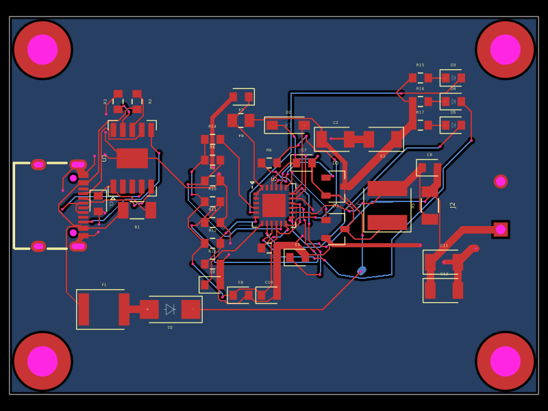
Schematic

import { AO3400A } from "./imports/AO3400A"
import { B5819W_SL } from "./imports/B5819W_SL"
import { CH224K } from "./imports/CH224K"
import { SS34 } from "./imports/SS34"

// USB-C PD charger for a 3S (12.6 V) Li-ion pack, 1.5 A.
// - CH224K asks the USB-C PD source for 15 V (CFG1 = 56k to GND).
// - TI BQ24610 standalone synchronous buck charger, simplified circuit from the
//   datasheet (SLUS892D, 10.2.2: no power path, no DPM).
//   VBAT = 2.1 V * (1 + 500k / 100k) = 12.6 V
//   ICHG = V(ISET1) / (20 * 10 mOhm); V(ISET1) = 3.3 V * 10k / 110k = 0.3 V -> 1.5 A
//   IPRE/ITERM = 1 A/V * V(ISET2); 3.3 V * 4.7k / 104.7k = 0.148 V -> ~150 mA
//   LC: 6.8 uH with 20 uF -> 13.6 kHz (datasheet wants 12-17 kHz)
// The pack needs its own 3S protection/balance board (BMS).

const BQ24610 = (props: { name: string; pcbX?: number; pcbY?: number; schX?: number; schY?: number; schSectionName?: string }) => (
  <chip
    {...props}
    manufacturerPartNumber="BQ24610RGER"
    footprint="qfn24_w4.6_h4.6_p0.5mm_pl0.6mm_pw0.25mm_thermalpad2.45mmx2.45mm"
    pinLabels={{
      pin1: "ACN",
      pin2: "ACP",
      pin3: "ACDRV",
      pin4: "CE",
      pin5: "STAT1",
      pin6: "TS",
      pin7: "TTC",
      pin8: "PG",
      pin9: "STAT2",
      pin10: "VREF",
      pin11: "ISET1",
      pin12: "VFB",
      pin13: "SRN",
      pin14: "SRP",
      pin15: "ISET2",
      pin16: "ACSET",
      pin17: "GND",
      pin18: "REGN",
      pin19: "LODRV",
      pin20: "PH",
      pin21: "HIDRV",
      pin22: "BTST",
      pin23: "BATDRV",
      pin24: "VCC",
      pin25: "EP",
    }}
    pinAttributes={{
      VCC: { requiresPower: true },
      GND: { requiresGround: true },
    }}
    schPinArrangement={{
      leftSide: {
        direction: "top-to-bottom",
        pins: ["VCC", "ACP", "ACN", "ACSET", "CE", "ISET1", "ISET2", "TS", "TTC", "VREF"],
      },
      rightSide: {
        direction: "top-to-bottom",
        pins: ["BTST", "HIDRV", "PH", "LODRV", "REGN", "SRP", "SRN", "VFB", "STAT1", "STAT2", "PG", "GND", "EP"],
      },
    }}
    noConnect={["ACDRV", "BATDRV"]}
  />
)

// L1: shielded power inductor on a 5040-size land pattern (two 1.6 x 4.2 mm pads, 3.6 mm apart)

export default () => (
  <board width="56mm" height="40mm">
    <schematicsection name="Input" displayName="USB-C PD input (15 V)" />
    <schematicsection name="Charger" displayName="BQ24610 3S buck charger" />
    <schematicsection name="Output" displayName="Battery + status" />

    {/* ---------- USB-C PD input ---------- */}
    <connector name="J1" pcbX={-22.3} pcbY={0} pcbRotation={-90} standard="usb_c" schSectionName="Input" schX={-14} schY={2} />
    <CH224K
      name="U1" pcbX={-15} pcbY={5}
      schSectionName="Input"
      schX={-9}
      schY={2}
      noConnect={["CFG2", "CFG3", "PG"]}
    />
    <resistor name="R1" pcbX={-14.5} pcbY={-0.5} schSectionName="Input" resistance="1k" footprint="1206" schX={-11} schY={5} schRotation={-90} />
    <capacitor name="C1" pcbX={-18.6} pcbY={0.2} schSectionName="Input" capacitance="1uF" footprint="0603" schX={-7} schY={5} schRotation={-90} pcbRotation={-90} maxDecouplingTraceLength="4mm" />
    <resistor name="R2" pcbX={-14.5} pcbY={11} pcbRotation={90} schSectionName="Input" resistance="10k" footprint="0603" schX={-11} schY={-1} schRotation={-90} />
    <resistor name="R3" pcbX={-16.5} pcbY={11} pcbRotation={90} schSectionName="Input" resistance="56k" footprint="0603" schX={-6} schY={-1} schRotation={-90} />
    <fuse name="F1" pcbX={-18} pcbY={-11} schSectionName="Input" currentRating="2A" voltageRating="30V" footprint="1812" schX={-11} schY={-5} schRotation={0} />
    <SS34 name="D1" pcbX={-11} pcbY={-11} pcbRotation={180} schSectionName="Input" schX={-8} schY={-5} schRotation={180} />
    <capacitor name="C2" pcbX={6.5} pcbY={7} schSectionName="Input" capacitance="10uF" maxVoltageRating="25V" footprint="1206" schX={-5} schY={-6} schRotation={-90} />
    <capacitor name="C3" pcbX={11.5} pcbY={7} pcbRotation={180} schSectionName="Input" capacitance="10uF" maxVoltageRating="25V" footprint="1206" schX={-4} schY={-6} schRotation={-90} />

    {/* ---------- BQ24610 charger ---------- */}
    <BQ24610 name="U2" pcbX={0} pcbY={0} schSectionName="Charger" schX={4} schY={0} />
    <resistor name="R4" pcbX={-3.5} pcbY={9} pcbRotation={180} schSectionName="Charger" resistance="10" footprint="0805" schX={0} schY={5} schRotation={-90} />
    <capacitor name="C4" pcbX={-3.5} pcbY={11.5} pcbRotation={180} schSectionName="Charger" capacitance="1uF" maxVoltageRating="25V" footprint="0603" schX={1} schY={6} schRotation={-90} />
    <capacitor name="C5" pcbX={2.5} pcbY={-5.5} schSectionName="Charger" capacitance="1uF" footprint="0603" schX={9} schY={-2} schRotation={-90} />
    <capacitor name="C6" pcbX={-3.5} pcbY={-9.5} schSectionName="Charger" capacitance="1uF" footprint="0603" schX={0} schY={-6.5} schRotation={-90} />
    <AO3400A name="Q1" pcbX={6.5} pcbY={2} pcbRotation={180} schSectionName="Charger" schX={11} schY={4} />
    <AO3400A name="Q2" pcbX={6.5} pcbY={-2.5} pcbRotation={180} schSectionName="Charger" schX={11} schY={1} />
    <B5819W_SL name="D2" pcbX={1.5} pcbY={8.5} schSectionName="Charger" schX={9} schY={5} />
    <capacitor name="C7" pcbX={3.2} pcbY={4.5} schSectionName="Charger" capacitance="100nF" footprint="0603" schX={10} schY={6} schOrientation="vertical" />
    <inductor name="L1" pcbX={12} pcbY={0} pcbRotation={90} schSectionName="Charger" inductance="6.8uH" footprint="res_p3.6mm_pw1.6mm_ph4.2mm" schX={14} schY={2} />
    <resistor name="R5" pcbX={16.5} pcbY={0} pcbRotation={90} schSectionName="Charger" resistance="10mOhm" footprint="1206" schX={17} schY={2} />
    <capacitor name="C8" pcbX={16.5} pcbY={4} schSectionName="Charger" capacitance="100nF" footprint="0603" schX={17} schY={4} schOrientation="vertical" />
    <resistor name="R6" pcbX={-0.5} pcbY={4.5} schSectionName="Charger" resistance="500k" footprint="0603" schX={7} schY={-5} schRotation={-90} />
    <resistor name="R7" pcbX={-0.5} pcbY={-4.5} schSectionName="Charger" resistance="100k" footprint="0603" schX={8} schY={-7} schRotation={-90} />
    <resistor name="R8" pcbX={-6.5} pcbY={4.8} schSectionName="Charger" resistance="100k" footprint="0603" schX={-1} schY={2} schRotation={-90} />
    <resistor name="R9" pcbX={-6.5} pcbY={2.6} schSectionName="Charger" resistance="10k" footprint="0603" schX={-1} schY={0} schRotation={-90} />
    <resistor name="R10" pcbX={-6.5} pcbY={0.4} schSectionName="Charger" resistance="100k" footprint="0603" schX={-1} schY={-2} schRotation={-90} />
    <resistor name="R11" pcbX={-6.5} pcbY={-1.8} schSectionName="Charger" resistance="4.7k" footprint="0603" schX={-1} schY={-3} schRotation={-90} />
    <resistor name="R12" pcbX={-6.5} pcbY={-4} schSectionName="Charger" resistance="10k" footprint="0603" schX={1} schY={-4} schRotation={-90} />
    <resistor name="R13" pcbX={-6.5} pcbY={-6.2} schSectionName="Charger" resistance="10k" footprint="0603" schX={1} schY={-5} schRotation={-90} />
    <capacitor name="C9" pcbX={-6.5} pcbY={-8.4} schSectionName="Charger" capacitance="56nF" footprint="0603" schX={2.5} schY={-6.5} schRotation={-90} />
    <resistor name="R14" pcbX={-6.5} pcbY={7} schSectionName="Charger" resistance="100k" footprint="0603" schX={-1} schY={4} schRotation={-90} />
    <capacitor name="C10" pcbX={-0.5} pcbY={-9.5} schSectionName="Charger" capacitance="1uF" footprint="0603" schX={1} schY={-6.5} schRotation={-90} />

    {/* ---------- Battery output + status ---------- */}
    <capacitor name="C11" pcbX={18} pcbY={-6} schSectionName="Output" capacitance="10uF" maxVoltageRating="25V" footprint="1206" schX={23} schY={0.5} schRotation={-90} />
    <capacitor name="C12" pcbX={18} pcbY={-9} schSectionName="Output" capacitance="10uF" maxVoltageRating="25V" footprint="1206" schX={24.5} schY={0.5} schRotation={-90} />
    <pinheader name="J2" pcbX={24} pcbY={0} pcbRotation={90} schSectionName="Output" pinCount={2} pitch="5.08mm" pinLabels={["BAT_P", "BAT_N"]} schX={27} schY={1} />
    <resistor name="R15" pcbX={15.5} pcbY={13.5} schSectionName="Output" resistance="10k" footprint="0603" schX={22.0} schY={-3.5} schRotation={-90} />
    <led name="D3" pcbX={19} pcbY={13.5} schSectionName="Output" color="red" footprint="0603" schX={22.0} schY={-5.6} schRotation={-90} supplierPartNumbers={{ jlcpcb: ["C2286"] }} />
    <resistor name="R16" pcbX={15.5} pcbY={11} schSectionName="Output" resistance="10k" footprint="0603" schX={23.6} schY={-3.5} schRotation={-90} />
    <led name="D4" pcbX={19} pcbY={11} schSectionName="Output" color="green" footprint="0603" schX={23.6} schY={-5.6} schRotation={-90} />
    <resistor name="R17" pcbX={15.5} pcbY={8.5} schSectionName="Output" resistance="10k" footprint="0603" schX={25.2} schY={-3.5} schRotation={-90} />
    <led name="D5" pcbX={19} pcbY={8.5} schSectionName="Output" color="green" footprint="0603" schX={25.2} schY={-5.6} schRotation={-90} />

    {[[-24.5, 16.5], [24.5, 16.5], [-24.5, -16.5], [24.5, -16.5]].map(([x, y], i) => (
      <platedhole key={i} name={`MH${i + 1}`} pcbX={x} pcbY={y} shape="circle" holeDiameter="3.2mm" outerDiameter="6mm" />
    ))}

    <copperpour connectsTo="net.GND" layer="bottom" clearance="0.25mm" />

    {/* USB-C and PD sink */}
    <trace thickness="0.8mm" from=".J1 > .VBUS1" to="net.VBUS" />
    <trace thickness="0.8mm" from=".J1 > .VBUS2" to="net.VBUS" />
    <trace thickness="0.8mm" from=".J1 > .GND1" to="net.GND" />
    <trace thickness="0.8mm" from=".J1 > .GND2" to="net.GND" />
    <trace from=".J1 > .SHELL1" to="net.GND" />
    <trace from=".J1 > .SHELL2" to="net.GND" />
    <trace from=".J1 > .CC1" to=".U1 > .CC1" />
    <trace from=".J1 > .CC2" to=".U1 > .CC2" />
    <trace from=".J1 > .DP1" to=".U1 > .DP" />
    <trace from=".J1 > .DP2" to=".U1 > .DP" />
    <trace from=".J1 > .DM1" to=".U1 > .DM" />
    <trace from=".J1 > .DM2" to=".U1 > .DM" />
    <trace from=".R1 > .pin1" to="net.VBUS" />
    <trace from=".R1 > .pin2" to=".U1 > .VDD" />
    <trace from=".C1 > .pin1" to=".U1 > .VDD" />
    <trace from=".C1 > .pin2" to="net.GND" />
    <trace from=".R2 > .pin1" to="net.VBUS" />
    <trace from=".R2 > .pin2" to=".U1 > .VBUS" />
    <trace from=".R3 > .pin1" to=".U1 > .CFG1" />
    <trace from=".R3 > .pin2" to="net.GND" />
    <trace from=".U1 > .GND" to="net.GND" />

    {/* Input protection: fuse + reverse-blocking Schottky */}
    <trace thickness="0.8mm" from=".F1 > .pin1" to="net.VBUS" />
    <trace thickness="0.8mm" from=".F1 > .pin2" to=".D1 > .anode" />
    <trace thickness="0.8mm" from=".D1 > .cathode" to="net.VIN" />
    <trace thickness="0.8mm" from=".C2 > .pin1" to="net.VIN" />
    <trace thickness="0.8mm" from=".C2 > .pin2" to="net.GND" />
    <trace thickness="0.8mm" from=".C3 > .pin1" to="net.VIN" />
    <trace thickness="0.8mm" from=".C3 > .pin2" to="net.GND" />

    {/* BQ24610 supply; no DPM: ACN/ACP tied to VCC, ACSET to VREF */}
    <trace from=".R4 > .pin1" to="net.VIN" />
    <trace from=".R4 > .pin2" to="net.VCC_CHG" />
    <trace from=".C4 > .pin1" to="net.VCC_CHG" />
    <trace from=".C4 > .pin2" to="net.GND" />
    <trace from=".U2 > .VCC" to="net.VCC_CHG" />
    <trace from=".U2 > .ACN" to="net.VCC_CHG" />
    <trace from=".U2 > .ACP" to="net.VCC_CHG" />
    <trace from=".U2 > .ACSET" to="net.VREF" />
    <trace from=".U2 > .GND" to="net.GND" />
    <trace from=".U2 > .EP" to="net.GND" />
    <trace from=".C5 > .pin1" to=".U2 > .REGN" />
    <trace from=".C5 > .pin2" to="net.GND" />
    <trace from=".C6 > .pin1" to="net.VREF" />
    <trace from=".C6 > .pin2" to="net.GND" />
    <trace from=".U2 > .VREF" to="net.VREF" />

    {/* Synchronous buck: Q1 high side, Q2 low side, bootstrap D2/C7 */}
    <trace thickness="0.8mm" from=".Q1 > .D" to="net.VIN" />
    <trace thickness="0.8mm" from=".Q1 > .S" to="net.PH" />
    <trace from=".Q1 > .G" to=".U2 > .HIDRV" />
    <trace thickness="0.8mm" from=".Q2 > .D" to="net.PH" />
    <trace thickness="0.8mm" from=".Q2 > .S" to="net.GND" />
    <trace from=".Q2 > .G" to=".U2 > .LODRV" />
    <trace from=".U2 > .PH" to="net.PH" />
    <trace from=".D2 > .anode" to=".U2 > .REGN" />
    <trace from=".D2 > .cathode" to=".U2 > .BTST" />
    <trace from=".C7 > .pin1" to=".U2 > .BTST" />
    <trace from=".C7 > .pin2" to="net.PH" />
    <trace thickness="0.8mm" from=".L1 > .pin1" to="net.PH" />
    <trace thickness="0.8mm" from=".L1 > .pin2" to="net.CHG_SRP" />

    {/* Charge-current sense R5 (10 mOhm) and battery side */}
    <trace thickness="0.8mm" from=".R5 > .pin1" to="net.CHG_SRP" />
    <trace thickness="0.8mm" from=".R5 > .pin2" to="net.BAT" />
    <trace from=".U2 > .SRP" to="net.CHG_SRP" />
    <trace from=".U2 > .SRN" to="net.BAT" />
    <trace from=".C8 > .pin1" to="net.CHG_SRP" />
    <trace from=".C8 > .pin2" to="net.BAT" />
    <trace thickness="0.8mm" from=".C11 > .pin1" to="net.BAT" />
    <trace thickness="0.8mm" from=".C11 > .pin2" to="net.GND" />
    <trace thickness="0.8mm" from=".C12 > .pin1" to="net.BAT" />
    <trace thickness="0.8mm" from=".C12 > .pin2" to="net.GND" />
    <trace thickness="0.8mm" from=".J2 > .BAT_P" to="net.BAT" />
    <trace thickness="0.8mm" from=".J2 > .BAT_N" to="net.GND" />

    {/* Programming: 12.6 V, 1.5 A, ~150 mA precharge/termination */}
    <trace from=".R6 > .pin1" to="net.BAT" />
    <trace from=".R6 > .pin2" to=".U2 > .VFB" />
    <trace from=".R7 > .pin1" to=".U2 > .VFB" />
    <trace from=".R7 > .pin2" to="net.GND" />
    <trace from=".R8 > .pin1" to="net.VREF" />
    <trace from=".R8 > .pin2" to=".U2 > .ISET1" />
    <trace from=".R9 > .pin1" to=".U2 > .ISET1" />
    <trace from=".R9 > .pin2" to="net.GND" />
    <trace from=".R10 > .pin1" to="net.VREF" />
    <trace from=".R10 > .pin2" to=".U2 > .ISET2" />
    <trace from=".R11 > .pin1" to=".U2 > .ISET2" />
    <trace from=".R11 > .pin2" to="net.GND" />
    {/* TS at 50% of VREF: inside the 37%-73.5% window (no pack thermistor) */}
    <trace from=".R12 > .pin1" to="net.VREF" />
    <trace from=".R12 > .pin2" to=".U2 > .TS" />
    <trace from=".R13 > .pin1" to=".U2 > .TS" />
    <trace from=".R13 > .pin2" to="net.GND" />
    <trace from=".C9 > .pin1" to=".U2 > .TTC" />
    <trace from=".C9 > .pin2" to="net.GND" />
    <trace from=".R14 > .pin1" to="net.VREF" />
    <trace from=".R14 > .pin2" to=".U2 > .CE" />
    <trace from=".C10 > .pin1" to="net.VREF" />
    <trace from=".C10 > .pin2" to="net.GND" />

    {/* Status LEDs on the open-drain outputs */}
    <trace from=".R15 > .pin1" to="net.VIN" />
    <trace from=".R15 > .pin2" to=".D3 > .anode" />
    <trace from=".D3 > .cathode" to=".U2 > .STAT1" />
    <trace from=".R16 > .pin1" to="net.VIN" />
    <trace from=".R16 > .pin2" to=".D4 > .anode" />
    <trace from=".D4 > .cathode" to=".U2 > .STAT2" />
    <trace from=".R17 > .pin1" to="net.VIN" />
    <trace from=".R17 > .pin2" to=".D5 > .anode" />
    <trace from=".D5 > .cathode" to=".U2 > .PG" />
  </board>
)
Related Packages
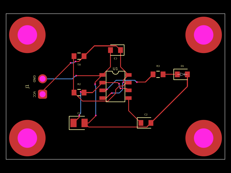 More from this authormukesh-dev-git/555-led-blinkerA 36×24 mm NE555-based astable LED blinker accepting 5–12 V through a 2-pin header, with timing RC components, red 1.5 Hz LED output, decoupling, and four M3 mounting holes.
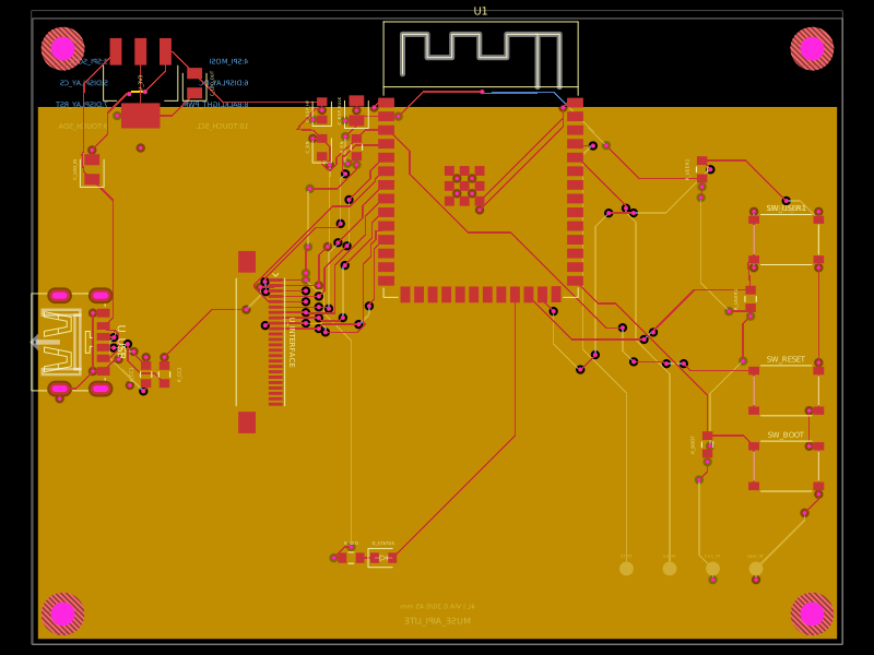 Discover something newShiboSoftwareDev/muse-aipi-lite-replacementA four-layer ESP32-S3 carrier board with USB‑C 5V input, AMS1117 3.3V regulation, FFC display/interface connector, status LED, reset/boot/user buttons, decoupling passives, test points, and ground/power planes.