mpsys/roveee-led-pcb
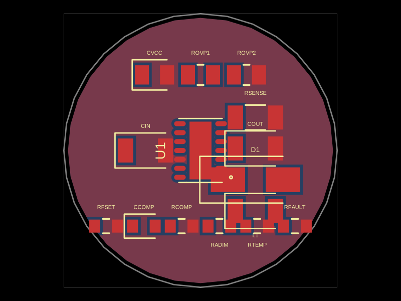
This code defines a surface-mount integrated circuit (TPS923655DMTR) used as a power management or driver component in a PCB, including its footprint, 3D model, and placement within a circuit with associated passive components and routing.
- Version
- 1.0.0
- License
- unset
- Stars
- 0
index.circuit.tsx
PCB
Schematic
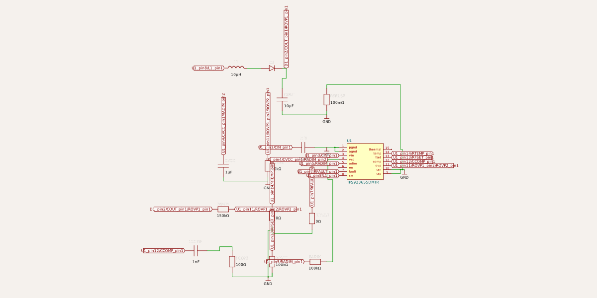
import { TPS923655DMTR } from "./imports/TPS923655DMTR"

export default () => {
  const BOARD_DIA = 19.9

  const CIRCLE_POINTS = 32
  const outline = Array.from({ length: CIRCLE_POINTS }, (_, i) => {
    const angle = (i / CIRCLE_POINTS) * Math.PI * 2
    return { x: (BOARD_DIA / 2) * Math.cos(angle), y: (BOARD_DIA / 2) * Math.sin(angle) }
  })

  return (
    <board
      width={`${BOARD_DIA}mm`}
      height={`${BOARD_DIA}mm`}
      outline={outline}
      layers={2}
      routingDisabled
    >
      <TPS923655DMTR name="U1" pcbX={0} pcbY={0} pcbRotation="90deg" />

      <group pcbFlex pcbFlexGap="0.5mm" pcbFlexDirection="column" pcbX={-4} pcbY={0}>
        <capacitor capacitance="10µF" footprint="1206" name="CIN" />
      </group>

      <group pcbFlex pcbFlexGap="0.5mm" pcbFlexDirection="column" pcbX={4} pcbY={-1}>
        <inductor inductance="10µH" footprint="1206" name="L1" />
        <diode name="D1" footprint="SMA" />
        <capacitor capacitance="10µF" footprint="1206" name="COUT" />
        <resistor resistance="0.1" footprint="1206" name="RSENSE" />
      </group>

      <group pcbFlex pcbFlexGap="0.5mm" pcbFlexDirection="row" pcbX={0} pcbY={5.5}>
        <capacitor capacitance="1µF" footprint="0805" name="CVCC" />
        <resistor resistance="150k" footprint="0805" name="ROVP1" />
        <resistor resistance="10k" footprint="0805" name="ROVP2" />
      </group>

      <group pcbFlex pcbFlexGap="0.3mm" pcbFlexDirection="row" pcbX={0} pcbY={-5.5}>
        <resistor resistance="100k" footprint="0603" name="RFSET" />
        <capacitor capacitance="1nF" footprint="0603" name="CCOMP" />
        <resistor resistance="100" footprint="0603" name="RCOMP" />
        <resistor resistance="100k" footprint="0603" name="RADIM" />
        <resistor resistance="0" footprint="0603" name="RTEMP" />
        <resistor resistance="0" footprint="0603" name="RFAULT" />
      </group>

      <copperpour connectsTo="net.GND" layer="top" clearance="0.15mm"
        padMargin="0.2mm" traceMargin="0.15mm" boardEdgeMargin="0.3mm" />
      <copperpour connectsTo="net.GND" layer="bottom" clearance="0.15mm"
        padMargin="0.2mm" traceMargin="0.15mm" boardEdgeMargin="0.3mm" />

      <trace from=".CIN > .pos" to=".U1 > .vin" />
      <trace from=".CIN > .neg" to="net.GND" />
      <trace from=".U1 > .sw" to=".L1 > .pin1" />
      <trace from=".L1 > .pin2" to=".D1 > .anode" />
      <trace from=".D1 > .cathode" to=".COUT > .pos" />
      <trace from=".COUT > .neg" to="net.GND" />
      <trace from=".RSENSE > .pin2" to="net.GND" />
      <trace from=".U1 > .csp" to=".RSENSE > .pin1" />
      <trace from=".U1 > .csn" to=".RSENSE > .pin2" />
      <trace from=".U1 > .vcc" to=".CVCC > .pos" />
      <trace from=".CVCC > .neg" to="net.GND" />
      <trace from=".U1 > .pgnd" to="net.GND" />
      <trace from=".U1 > .agnd" to="net.GND" />
      <trace from=".U1 > .fset" to=".RFSET > .pin1" />
      <trace from=".RFSET > .pin2" to="net.GND" />
      <trace from=".U1 > .comp" to=".CCOMP > .pos" />
      <trace from=".CCOMP > .neg" to=".RCOMP > .pin1" />
      <trace from=".RCOMP > .pin2" to="net.GND" />
      <trace from=".COUT > .pos" to=".ROVP1 > .pin1" />
      <trace from=".ROVP1 > .pin2" to=".U1 > .ovp" />
      <trace from=".U1 > .ovp" to=".ROVP2 > .pin1" />
      <trace from=".ROVP2 > .pin2" to="net.GND" />
      <trace from=".U1 > .temp" to=".RTEMP > .pin1" />
      <trace from=".RTEMP > .pin2" to="net.GND" />
      <trace from=".U1 > .fault" to=".RFAULT > .pin1" />
      <trace from=".RFAULT > .pin2" to="net.GND" />
      <trace from=".U1 > .adim" to=".RADIM > .pin1" />
      <trace from=".RADIM > .pin2" to=".U1 > .vcc" />
    </board>
  )
}