mohan-bee/soil-final
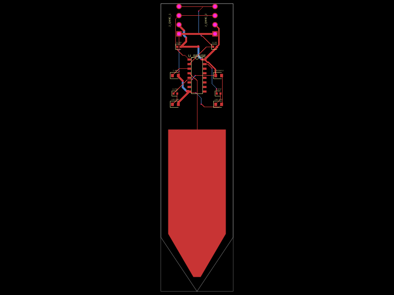
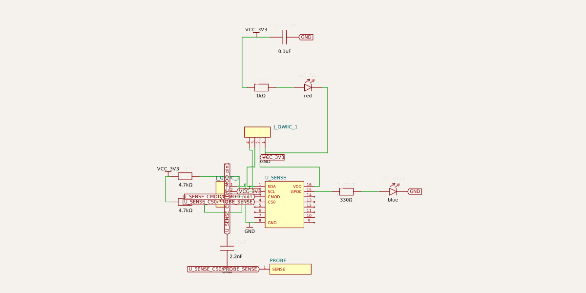
This code defines a printed circuit board (PCB) featuring a sensor chip with associated decoupling capacitors, resistors, indicator LEDs with current-limiting resistors, pin headers for external connections, and a custom spear-shaped probe pad.
- Version
- 0.0.1
- License
- unset
- Stars
- 0
index.tsx
PCB
Schematic
import React from "react"

export default () => (
  <board
    width="20mm"
    height="80mm"
    outline={[
      { x: -10, y: 40 },
      { x: 10, y: 40 },
      { x: 10, y: -25 },  /* Start of the angle */
      { x: 0, y: -40 },   /* The Pointed Tip */
      { x: -10, y: -25 }, /* Start of the angle */
    ]}
  >

    {/* 1. GLOBAL NETS */}
    <net name="VCC_3V3" isPowerNet={true} />
    <net name="GND" isGroundNet={true} />


    <pinheader name="J_QWIIC_1" pinCount={4} pcbX={-5} pcbY={35.4} pcbRotation={90} />
    <pinheader name="J_QWIIC_2" pinCount={4} pcbX={5} pcbY={35.4} pcbRotation={90} />

    <chip
      name="U_SENSE"
      footprint="soic16"
      pcbX={0}
      pcbY={20}
      pinLabels={{
        pin1: "SDA", pin2: "SCL", pin3: "CMOD", pin4: "CS0",
        pin8: "GND", pin15: "GPO0", pin16: "VDD"
      }}
    />

    <capacitor name="C_MOD" capacitance="2.2nF" footprint="0603" pcbX={-6} pcbY={20} />
    <capacitor name="C_DECOUPLE" capacitance="0.1uF" footprint="0603" pcbX={6} pcbY={20} />

    <resistor name="R_SDA" resistance="4.7k" footprint="0402" pcbX={-5} pcbY={28} />
    <resistor name="R_SCL" resistance="4.7k" footprint="0402" pcbX={5} pcbY={28} />

    <led name="LED_PWR" color="red" footprint="0603" pcbX={-6} pcbY={12} />
    <resistor name="R_PWR" resistance="1k" footprint="0402" pcbX={-6} pcbY={15} />

    <led name="LED_STAT" color="blue" footprint="0603" pcbX={6} pcbY={12} />
    <resistor name="R_STAT" resistance="330" footprint="0402" pcbX={6} pcbY={15} />

    <chip
      name="PROBE"
      pcbX={0}
      pcbY={0}
      pinLabels={{ pin1: "SENSE" }}
      footprint={
        <footprint>
          {/* 1. THE ANCHOR PAD: A standard rectangle the router can easily find and snap to! */}
          <smtpad
            portHints={["pin1"]}
            pcbX={0} pcbY={-5}
            width="2mm" height="2mm" shape="rect" layer="top"
          />

          {/* 2. THE COPPER FILL: The custom polygon that gives us the spear shape */}
          <smtpad
            portHints={["pin1"]}
            pcbX={0} pcbY={0}
            layer="top" shape="polygon"
            points={[
              { x: -8, y: 5 },
              { x: 8, y: 5 },
              { x: 8, y: -24 },
              { x: 1, y: -36 },
              { x: -1, y: -36 },
              { x: -8, y: -24 },
            ]}
          />

          {/* 3. THE COURTYARD: A custom 1mm safety buffer hugging the spear! */}
         <courtyardoutline
            outline={[
              { x: -9, y: 6 },
              { x: 9, y: 6 },
              { x: 9, y: -24 },
              { x: 2, y: -37 },
              { x: -2, y: -37 },
              { x: -9, y: -24 },
            ]}
          />
        </footprint>
      }
    />


    <trace from=".J_QWIIC_1 > .pin1" to="net.GND" thickness="0.6mm" />
    <trace from=".J_QWIIC_1 > .pin2" to="net.VCC_3V3" thickness="0.6mm" />
    <trace from=".J_QWIIC_2 > .pin1" to="net.GND" thickness="0.6mm" />
    <trace from=".J_QWIIC_2 > .pin2" to="net.VCC_3V3" thickness="0.6mm" />

    <trace from=".U_SENSE > .VDD" to="net.VCC_3V3" thickness="0.4mm" />
    <trace from=".U_SENSE > .GND" to="net.GND" thickness="0.4mm" />

    <trace from=".C_DECOUPLE > .pin1" to="net.VCC_3V3" />
    <trace from=".C_DECOUPLE > .pin2" to="net.GND" />

    <trace from=".J_QWIIC_1 > .pin3" to=".J_QWIIC_2 > .pin3" />
    <trace from=".J_QWIIC_1 > .pin4" to=".J_QWIIC_2 > .pin4" />
    <trace from=".J_QWIIC_1 > .pin3" to=".U_SENSE > .SDA" />
    <trace from=".J_QWIIC_1 > .pin4" to=".U_SENSE > .SCL" />

    <trace from=".U_SENSE > .SDA" to=".R_SDA > .pin1" />
    <trace from=".R_SDA > .pin2" to="net.VCC_3V3" />
    <trace from=".U_SENSE > .SCL" to=".R_SCL > .pin1" />
    <trace from=".R_SCL > .pin2" to="net.VCC_3V3" />

    <trace from="net.VCC_3V3" to=".R_PWR > .pin1" />
    <trace from=".R_PWR > .pin2" to=".LED_PWR > .pos" />
    <trace from=".LED_PWR > .neg" to="net.GND" />

    <trace from=".U_SENSE > .GPO0" to=".R_STAT > .pin1" />
    <trace from=".R_STAT > .pin2" to=".LED_STAT > .pos" />
    <trace from=".LED_STAT > .neg" to="net.GND" />

    <trace from=".U_SENSE > .CMOD" to=".C_MOD > .pin1" />
    <trace from=".C_MOD > .pin2" to="net.GND" />

    <trace from=".U_SENSE > .pin4" to=".PROBE > .SENSE" thickness="0.2mm" />

  </board>
)
Related Packages
 More from this authormohan-bee/esp32-c3This hardware design integrates an ESP32-C3 microcontroller, a USB-C connector, a power management IC (AP2112-3.3V regulator), a USB-to-Serial converter (CH340C), several resistors, capacitors, and user-accessible headers to facilitate USB communication, power regulation, and general I/O interfacing.
 Similar packagetinsangbeeping/my_led_testingThis code defines a React component that creates an electronic module with an 8-pin microcontroller (like ATMEGA328P) connected to an external 2-pin header, including an internal signal path with a resistor and LED for visual indication, plus optional decoupling capacitor.
 Discover something newAnasSarkiz/NEMA14_CH32X035G8U6A NEMA stepper motor is shown with proposed M3 screws/spacers, four wired motor leads and splices, and a JST SHR-04V-S connector.