mohan-bee/relay-module
A tscircuit package created by mohan-bee.
- Version
- 1.0.0
- License
- unset
- Stars
- 0
index.circuit.tsx
PCB
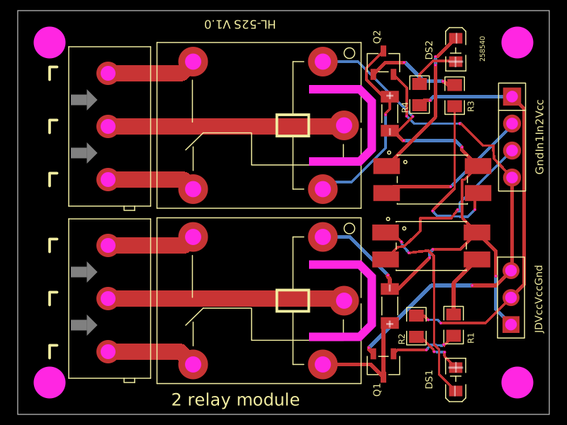
Schematic

import { Fragment } from "react"
import { SRD_05VDC_SL_C as Relay } from "./components/jlc-relay-c35449/SRD_05VDC_SL_C"
import { KF301_5_0_3P as Terminal } from "./components/jlc-terminal-c474882/KF301_5_0_3P"
import { PC817X3CSP9F as Optocoupler } from "./components/jlc-PC817X3CSP9F-C41807"
import { S8050_J3Y_RANGE_200_350_ as Driver } from "./components/jlc-S8050-C2146"
import { LL4148 as FlybackDiode } from "./components/jlc-LL4148-C9808"
import { A_0805W8F1001T5E as Resistor1k } from "./components/C17513_0805_1k"
import { NCD0805R1 as RedLED } from "./components/C84256_Red0805"
import { B_2100S03P_A110 as Header3 } from "./components/C124376_Header1x03"
import { B_2100S04P_A110 as Header4 } from "./components/C124378_Header1x04"

// Photo reconstruction of Quartz MOD-QC0518, HL-52S V1.0. Board dimensions are unverified.
// All physical components retain their unmodified JLCPCB-imported footprints and CAD.
export const mechanical = { width: 50, height: 38, thickness: 1.6, holeDiameter: 3, holePitchX: 44, holePitchY: 32 }

function Silk({ text, x, y, size = 1, rotation = 0 }: { text: string; x: number; y: number; size?: number; rotation?: number }) {
  return <silkscreentext text={text} pcbX={x} pcbY={y} fontSize={size} pcbRotation={rotation}
    anchorAlignment="center" pcbStyle={{ silkscreenTextVisibility: "visible" }} />
}

function Channel({ ch, y, sy }: { ch: 1 | 2; y: number; sy: number }) {
  const lower = ch === 1
  const section = `channel${ch}`
  const inputR = ch * 2
  const baseR = ch * 2 - 1
  const rx = lower ? 12.5 : 12.8
  const ry = lower ? -10.7 : 11.1
  const dy = lower ? -8.8 : 9.3
  const ly = lower ? -15.7 : 15.3
  return <>
    <schematicsection name={section} displayName={`Channel ${ch} — active low`} />
    {/* Native C35449 pins: 1/4 coil, 5 COM, 3 NC, 2 NO. Rotation puts coil on right. */}
    <Relay name={`K${ch}`} pcbX={-1.4} pcbY={y} pcbRotation={180}
      schX={12} schY={sy} schSectionName={section}
      connections={{ pin1: "net.JDVCC", pin4: `net.COIL${ch}` }} />
    <Terminal name={`J${ch}`} pcbX={-16.5} pcbY={lower ? -8.1 : 8.1} pcbRotation={270}
      schX={18} schY={sy} schSectionName={section} />
    {[["NO", 2, 1], ["COM", 5, 2], ["NC", 3, 3]].map(([net, relayPin, terminalPin]) =>
      <Fragment key={net}><trace path={[`.K${ch} > .pin${relayPin}`, `.J${ch} > .pin${terminalPin}`, `net.${net}${ch}`]} thickness={1.5} /></Fragment>)}
    <Optocoupler name={`U${ch}`} pcbX={lower ? 13.9 : 14} pcbY={lower ? -3.15 : 3.1}
      schX={-4} schY={sy} schSectionName={section}
      connections={{ AN: `net.OPTO_A${ch}`, CAT: `net.IN${ch}`, EM: `net.OPTO_E${ch}`, COL: "net.JDVCC" }} />
    <Resistor1k name={`R${inputR}`} pcbX={rx} pcbY={ry} pcbRotation={lower ? -90 : 90}
      schX={-12} schY={sy + 1} schRotation={-90} schSectionName={section}
      connections={{ pin1: "net.VCC", pin2: `net.LED_A${ch}` }} />
    <RedLED name={`DS${ch}`} color="red" pcbX={16.2} pcbY={ly} pcbRotation={lower ? 90 : -90}
      schX={-12} schY={sy - 1} schRotation={-90} schSectionName={section}
      connections={{ pin2: `net.LED_A${ch}`, pin1: `net.OPTO_A${ch}` }} />
    <Resistor1k name={`R${baseR}`} pcbX={lower ? 16 : 16.1} pcbY={lower ? -10.6 : 11} pcbRotation={lower ? -90 : 90}
      schX={1} schY={sy - 1} schSectionName={section}
      connections={{ pin1: `net.OPTO_E${ch}`, pin2: `net.BASE${ch}` }} />
    <Driver name={`Q${ch}`} pcbX={9.4} pcbY={lower ? -14.4 : 14.1} pcbRotation={lower ? 90 : -90}
      schX={6} schY={sy - 1} schSectionName={section}
      connections={{ B: `net.BASE${ch}`, E: "net.GND", C: `net.COIL${ch}` }} />
    <FlybackDiode name={`D${ch}`} pcbX={10} pcbY={dy} pcbRotation={lower ? -90 : 90}
      schX={7} schY={sy + 4} schRotation={180} schSectionName={section}
      connections={{ pin1: "net.JDVCC", pin2: `net.COIL${ch}` }} />
    {/* Slot geometry is photo-derived, not an original manufacturing drawing. */}
    <cutout shape="polygon" points={[
      { x: 2.4, y: y + 3.8 }, { x: 7.3, y: y + 3.8 }, { x: 8.7, y: y + 2.4 },
      { x: 8.7, y: y - 2.4 }, { x: 7.3, y: y - 3.8 }, { x: 2.4, y: y - 3.8 },
      { x: 2.4, y: y - 3 }, { x: 7, y: y - 3 }, { x: 7.9, y: y - 2.1 },
      { x: 7.9, y: y + 2.1 }, { x: 7, y: y + 3 }, { x: 2.4, y: y + 3 },
    ]} />
    <Silk text={`Q${ch}`} x={8.8} y={lower ? -16.7 : 16.5} size={0.9} rotation={90} />
    <Silk text={`D${ch}`} x={8.3} y={dy} size={0.9} rotation={90} />
    <Silk text={`DS${ch}`} x={13.7} y={ly} size={0.9} rotation={90} />
    <Silk text={`R${inputR}`} x={rx - 1.4} y={ry - 1.2} size={0.8} rotation={90} />
    <Silk text={`R${baseR}`} x={17.6} y={ry - 1.1} size={0.8} rotation={90} />
    {[-5, 0, 5].map((offset, i) => <Fragment key={i}><silkscreenpath strokeWidth={0.25} route={[
      { x: -21.3, y: (lower ? -8.1 : 8.1) + offset + 0.6 },
      { x: -22, y: (lower ? -8.1 : 8.1) + offset + 0.6 },
      { x: -22, y: (lower ? -8.1 : 8.1) + offset - 0.6 },
    ]} /></Fragment>)}
  </>
}

export default function RelayModule() {
  return <board width={mechanical.width} height={mechanical.height} thickness={mechanical.thickness}
    layers={2} solderMaskColor="black" title="HL-52S V1.0 — JLCPCB-imported reconstruction"
    autorouter="auto-local" defaultTraceWidth={0.35} minTraceWidth={0.25}
    schMaxTraceDistance={5} pcbStyle={{ silkscreenTextVisibility: "hidden" }}>
    <schematicsection name="interface" displayName="Logic and relay supplies" />
    <net name="VCC" /><net name="JDVCC" /><net name="GND" />
    <Header4 name="JIN" pcbX={21.5} pcbY={7.1} pcbRotation={-90}
      schX={-12} schY={17} schSectionName="interface"
      connections={{ pin1: "net.VCC", pin2: "net.IN2", pin3: "net.IN1", pin4: "net.GND" }} />
    <Header3 name="JPOWER" pcbX={21.4} pcbY={-8} pcbRotation={90}
      schX={-3} schY={17} schSectionName="interface"
      connections={{ pin1: "net.JDVCC", pin2: "net.VCC", pin3: "net.GND" }} />
    <Channel ch={1} y={-8.3} sy={-9} />
    <Channel ch={2} y={8.2} sy={6} />
    {[-22, 22].flatMap((x) => [-16, 16].map((y) => <Fragment key={`${x},${y}`}><hole pcbX={x} pcbY={y} diameter={mechanical.holeDiameter} /></Fragment>))}
    <Silk text="2 relay module" x={-4.5} y={-17.6} size={1.6} />
    <Silk text="HL-52S V1.0" x={-4.1} y={17.7} size={1.1} rotation={180} />
    <Silk text="GndIn1In2Vcc" x={24.1} y={7.1} size={1} rotation={90} />
    <Silk text="JDVccVccGnd" x={24} y={-8.2} size={0.95} rotation={90} />
    <Silk text="258540" x={18.7} y={15.4} size={0.65} rotation={90} />
  </board>
}
Related Packages
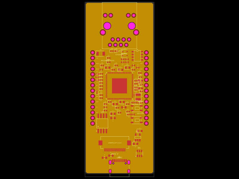 More from this authormohan-bee/RV1106G2This code defines a detailed hardware schematic with schematic symbols, footprints, and 3D models for various electronic components including microcontrollers, voltage regulators, connectors, and passive parts, designed for PCB layout and routing.
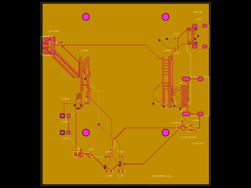 Discover something newgokul/cm4-media-carrier