mohan-bee/pcb
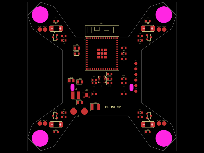
This circuit integrates an ESP32 microcontroller with an IMU sensor and power management components, using multiple capacitors, resistors, and MOSFETs for motor control, while managing power supply and battery connections.
- Version
- 1.0.0
- License
- unset
- Stars
- 0
preview/pcb.svg
PCB
Schematic
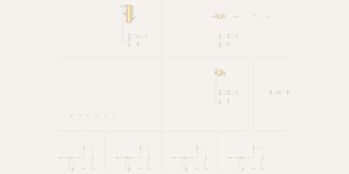
<svg xmlns="http://www.w3.org/2000/svg" width="800" height="600"><style></style><rect class="boundary" x="0" y="0" fill="#000" width="800" height="600" data-type="pcb_background" data-pcb-layer="global"/><rect class="pcb-boundary" fill="none" stroke="#fff" stroke-width="0.3" x="108.57142857142856" y="8.571428571428555" width="582.8571428571429" height="582.8571428571429" data-type="pcb_boundary" data-pcb-layer="global"/><path class="pcb-board" d="M 297.1428571428571 145.71428571428572 L 502.8571428571429 145.71428571428572 L 588.5714285714286 25.714285714285722 L 640 8.571428571428555 L 691.4285714285714 60 L 674.2857142857142 111.42857142857144 L 554.2857142857142 197.14285714285714 L 554.2857142857142 402.8571428571429 L 674.2857142857142 488.57142857142856 L 691.4285714285714 540 L 640 591.4285714285714 L 588.5714285714286 574.2857142857142 L 502.8571428571429 454.2857142857143 L 297.1428571428571 454.2857142857143 L 211.42857142857144 574.2857142857142 L 160 591.4285714285714 L 108.57142857142856 540 L 125.71428571428572 488.57142857142856 L 245.71428571428572 402.8571428571429 L 245.71428571428572 197.14285714285714 L 125.71428571428572 111.42857142857144 L 108.57142857142856 60 L 160 8.571428571428555 L 211.42857142857144 25.714285714285722 Z" fill="none" stroke="rgba(255, 255, 255, 0.5)" stroke-width="0.8571428571428572" data-type="pcb_board" data-pcb-layer="board"/><rect class="pcb-pad" fill="rgb(200, 52, 52)" x="336.7849154285714" y="157.2850577142857" width="6.857129142857143" height="3.4285645714285713" data-type="pcb_smtpad" data-pcb-layer="top" data-pad-name="U1.GND1" data-pad-net-name="GND"/><rect class="pcb-pad" fill="rgb(200, 52, 52)" x="336.7849154285714" y="164.5697777142857" width="6.857129142857143" height="3.4285645714285713" data-type="pcb_smtpad" data-pcb-layer="top" data-pad-name="U1.GND2" data-pad-net-name="GND"/><rect class="pcb-pad" fill="rgb(200, 52, 52)" x="336.7849154285714" y="171.85667485714285" width="6.857129142857143" height="3.4285645714285713" data-type="pcb_smtpad" data-pcb-layer="top" data-pad-name="U1.3V3" data-pad-net-name="V3V3"/><rect class="pcb-pad" fill="rgb(200, 52, 52)" x="336.7849154285714" y="179.14139485714284" width="6.857129142857143" height="3.4285645714285713" data-type="pcb_smtpad" data-pcb-layer="top" data-pad-name="U1.IO0" data-pad-net-name="BOOT"/><rect class="pcb-pad" fill="rgb(200, 52, 52)" x="336.7849154285714" y="186.42829200000003" width="6.857129142857143" height="3.4285645714285713" data-type="pcb_smtpad" data-pcb-layer="top" data-pad-name="U1.IO1" data-pad-net-name="VBAT_ADC"/><rect class="pcb-pad" fill="rgb(200, 52, 52)" x="336.7849154285714" y="193.71301200000002" width="6.857129142857143" height="3.4285645714285713" data-type="pcb_smtpad" data-pcb-layer="top" data-pad-name="U1.IO2"/><rect class="pcb-pad" fill="rgb(200, 52, 52)" x="336.7849154285714" y="200.99990914285715" width="6.857129142857143" height="3.4285645714285713" data-type="pcb_smtpad" data-pcb-layer="top" data-pad-name="U1.IO3"/><rect class="pcb-pad" fill="rgb(200, 52, 52)" x="336.7849154285714" y="208.28462914285714" width="6.857129142857143" height="3.4285645714285713" data-type="pcb_smtpad" data-pcb-layer="top" data-pad-name="U1.IO4"/><rect class="pcb-pad" fill="rgb(200, 52, 52)" x="336.7849154285714" y="215.56934914285713" width="6.857129142857143" height="3.4285645714285713" data-type="pcb_smtpad" data-pcb-layer="top" data-pad-name="U1.IO5"/><rect class="pcb-pad" fill="rgb(200, 52, 52)" x="336.7849154285714" y="222.85624628571426" width="6.857129142857143" height="3.4285645714285713" data-type="pcb_smtpad" data-pcb-layer="top" data-pad-name="U1.IO6"/><rect class="pcb-pad" fill="rgb(200, 52, 52)" x="336.7849154285714" y="230.14096628571428" width="6.857129142857143" height="3.4285645714285713" data-type="pcb_smtpad" data-pcb-layer="top" data-pad-name="U1.IO7"/><rect class="pcb-pad" fill="rgb(200, 52, 52)" x="336.7849154285714" y="237.42786342857144" width="6.857129142857143" height="3.4285645714285713" data-type="pcb_smtpad" data-pcb-layer="top" data-pad-name="U1.IO8" data-pad-net-name="IMU_CS"/><rect class="pcb-pad" fill="rgb(200, 52, 52)" x="336.7849154285714" y="244.71258342857143" width="6.857129142857143" height="3.4285645714285713" data-type="pcb_smtpad" data-pcb-layer="top" data-pad-name="U1.IO9"/><rect class="pcb-pad" fill="rgb(200, 52, 52)" x="336.7849154285714" y="251.99948057142856" width="6.857129142857143" height="3.4285645714285713" data-type="pcb_smtpad" data-pcb-layer="top" data-pad-name="U1.IO10"/><rect class="pcb-pad" fill="rgb(200, 52, 52)" x="336.7849154285714" y="259.2842005714286" width="6.857129142857143" height="3.4285645714285713" data-type="pcb_smtpad" data-pcb-layer="top" data-pad-name="U1.IO11" data-pad-net-name="IMU_MOSI"/><rect class="pcb-pad" fill="rgb(200, 52, 52)" x="347.2861462857143" y="266.785764" width="3.4285645714285713" height="6.857129142857143" data-type="pcb_smtpad" data-pcb-layer="top" data-pad-name="U1.IO12" data-pad-net-name="IMU_SCK"/><rect class="pcb-pad" fill="rgb(200, 52, 52)" x="354.5708662857143" y="266.785764" width="3.4285645714285713" height="6.857129142857143" data-type="pcb_smtpad" data-pcb-layer="top" data-pad-name="U1.IO13" data-pad-net-name="IMU_MISO"/><rect class="pcb-pad" fill="rgb(200, 52, 52)" x="361.85776342857145" y="266.785764" width="3.4285645714285713" height="6.857129142857143" data-type="pcb_smtpad" data-pcb-layer="top" data-pad-name="U1.IO14" data-pad-net-name="IMU_INT"/><rect class="pcb-pad" fill="rgb(200, 52, 52)" x="369.14248342857144" y="266.785764" width="3.4285645714285713" height="6.857129142857143" data-type="pcb_smtpad" data-pcb-layer="top" data-pad-name="U1.IO15"/><rect class="pcb-pad" fill="rgb(200, 52, 52)" x="376.4293805714286" y="266.785764" width="3.4285645714285713" height="6.857129142857143" data-type="pcb_smtpad" data-pcb-layer="top" data-pad-name="U1.IO16"/><rect class="pcb-pad" fill="rgb(200, 52, 52)" x="383.7141005714286" y="266.785764" width="3.4285645714285713" height="6.857129142857143" data-type="pcb_smtpad" data-pcb-layer="top" data-pad-name="U1.IO17"/><rect class="pcb-pad" fill="rgb(200, 52, 52)" x="391.00099771428575" y="266.785764" width="3.4285645714285713" height="6.857129142857143" data-type="pcb_smtpad" data-pcb-layer="top" data-pad-name="U1.IO18"/><rect class="pcb-pad" fill="rgb(200, 52, 52)" x="398.28571771428574" y="266.785764" width="3.4285645714285713" height="6.857129142857143" data-type="pcb_smtpad" data-pcb-layer="top" data-pad-name="U1.IO19"/><rect class="pcb-pad" fill="rgb(200, 52, 52)" x="405.57043771428573" y="266.785764" width="3.4285645714285713" height="6.857129142857143" data-type="pcb_smtpad" data-pcb-layer="top" data-pad-name="U1.IO20"/><rect class="pcb-pad" fill="rgb(200, 52, 52)" x="412.85733485714286" y="266.785764" width="3.4285645714285713" height="6.857129142857143" data-type="pcb_smtpad" data-pcb-layer="top" data-pad-name="U1.IO21"/><rect class="pcb-pad" fill="rgb(200, 52, 52)" x="420.14205485714285" y="266.785764" width="3.4285645714285713" height="6.857129142857143" data-type="pcb_smtpad" data-pcb-layer="top" data-pad-name="U1.IO26"/><rect class="pcb-pad" fill="rgb(200, 52, 52)" x="427.42895200000004" y="266.785764" width="3.4285645714285713" height="6.857129142857143" data-type="pcb_smtpad" data-pcb-layer="top" data-pad-name="U1.IO47"/><rect class="pcb-pad" fill="rgb(200, 52, 52)" x="434.71367200000003" y="266.785764" width="3.4285645714285713" height="6.857129142857143" data-type="pcb_smtpad" data-pcb-layer="top" data-pad-name="U1.IO33"/><rect class="pcb-pad" fill="rgb(200, 52, 52)" x="442.00056914285716" y="266.785764" width="3.4285645714285713" height="6.857129142857143" data-type="pcb_smtpad" data-pcb-layer="top" data-pad-name="U1.IO34"/><rect class="pcb-pad" fill="rgb(200, 52, 52)" x="449.28528914285715" y="266.785764" width="3.4285645714285713" height="6.857129142857143" data-type="pcb_smtpad" data-pcb-layer="top" data-pad-name="U1.IO48"/><rect class="pcb-pad" fill="rgb(200, 52, 52)" x="456.3579554285714" y="259.2842005714286" width="6.857129142857143" height="3.4285645714285713" data-type="pcb_smtpad" data-pcb-layer="top" data-pad-name="U1.IO35"/><rect class="pcb-pad" fill="rgb(200, 52, 52)" x="456.3579554285714" y="251.99948057142856" width="6.857129142857143" height="3.4285645714285713" data-type="pcb_smtpad" data-pcb-layer="top" data-pad-name="U1.IO36"/><rect class="pcb-pad" fill="rgb(200, 52, 52)" x="456.3579554285714" y="244.71258342857143" width="6.857129142857143" height="3.4285645714285713" data-type="pcb_smtpad" data-pcb-layer="top" data-pad-name="U1.IO37"/><rect class="pcb-pad" fill="rgb(200, 52, 52)" x="456.3579554285714" y="237.42786342857144" width="6.857129142857143" height="3.4285645714285713" data-type="pcb_smtpad" data-pcb-layer="top" data-pad-name="U1.IO38"/><rect class="pcb-pad" fill="rgb(200, 52, 52)" x="456.3579554285714" y="230.14096628571428" width="6.857129142857143" height="3.4285645714285713" data-type="pcb_smtpad" data-pcb-layer="top" data-pad-name="U1.IO39" data-pad-net-name="M1_PWM"/><rect class="pcb-pad" fill="rgb(200, 52, 52)" x="456.3579554285714" y="222.85624628571426" width="6.857129142857143" height="3.4285645714285713" data-type="pcb_smtpad" data-pcb-layer="top" data-pad-name="U1.IO40" data-pad-net-name="M2_PWM"/><rect class="pcb-pad" fill="rgb(200, 52, 52)" x="456.3579554285714" y="215.56934914285713" width="6.857129142857143" height="3.4285645714285713" data-type="pcb_smtpad" data-pcb-layer="top" data-pad-name="U1.IO41" data-pad-net-name="M3_PWM"/><rect class="pcb-pad" fill="rgb(200, 52, 52)" x="456.3579554285714" y="208.28462914285714" width="6.857129142857143" height="3.4285645714285713" data-type="pcb_smtpad" data-pcb-layer="top" data-pad-name="U1.IO42" data-pad-net-name="M4_PWM"/><rect class="pcb-pad" fill="rgb(200, 52, 52)" x="456.3579554285714" y="200.99990914285715" width="6.857129142857143" height="3.4285645714285713" data-type="pcb_smtpad" data-pcb-layer="top" data-pad-name="U1.TXD0" data-pad-net-name="UART_TX"/><rect class="pcb-pad" fill="rgb(200, 52, 52)" x="456.3579554285714" y="193.71301200000002" width="6.857129142857143" height="3.4285645714285713" data-type="pcb_smtpad" data-pcb-layer="top" data-pad-name="U1.RXD0" data-pad-net-name="UART_RX"/><rect class="pcb-pad" fill="rgb(200, 52, 52)" x="456.3579554285714" y="186.42829200000003" width="6.857129142857143" height="3.4285645714285713" data-type="pcb_smtpad" data-pcb-layer="top" data-pad-name="U1.IO45"/><rect class="pcb-pad" fill="rgb(200, 52, 52)" x="456.3579554285714" y="179.14139485714284" width="6.857129142857143" height="3.4285645714285713" data-type="pcb_smtpad" data-pcb-layer="top" data-pad-name="U1.GND3" data-pad-net-name="GND"/><rect class="pcb-pad" fill="rgb(200, 52, 52)" x="456.3579554285714" y="171.85667485714285" width="6.857129142857143" height="3.4285645714285713" data-type="pcb_smtpad" data-pcb-layer="top" data-pad-name="U1.GND4" data-pad-net-name="GND"/><rect class="pcb-pad" fill="rgb(200, 52, 52)" x="456.3579554285714" y="164.5697777142857" width="6.857129142857143" height="3.4285645714285713" data-type="pcb_smtpad" data-pcb-layer="top" data-pad-name="U1.IO46"/><rect class="pcb-pad" fill="rgb(200, 52, 52)" x="456.3579554285714" y="157.2850577142857" width="6.857129142857143" height="3.4285645714285713" data-type="pcb_smtpad" data-pcb-layer="top" data-pad-name="U1.EN" data-pad-net-name="EN"/><rect class="pcb-pad" fill="rgb(200, 52, 52)" x="449.28528914285715" y="146.35710685714284" width="3.4285645714285713" height="6.857129142857143" data-type="pcb_smtpad" data-pcb-layer="top" data-pad-name="U1.GND5" data-pad-net-name="GND"/><rect class="pcb-pad" fill="rgb(200, 52, 52)" x="442.00056914285716" y="146.35710685714284" width="3.4285645714285713" height="6.857129142857143" data-type="pcb_smtpad" data-pcb-layer="top" data-pad-name="U1.GND6" data-pad-net-name="GND"/><rect class="pcb-pad" fill="rgb(200, 52, 52)" x="434.71367200000003" y="146.35710685714284" width="3.4285645714285713" height="6.857129142857143" data-type="pcb_smtpad" data-pcb-layer="top" data-pad-name="U1.GND7" data-pad-net-name="GND"/><rect class="pcb-pad" fill="rgb(200, 52, 52)" x="427.42895200000004" y="146.35710685714284" width="3.4285645714285713" height="6.857129142857143" data-type="pcb_smtpad" data-pcb-layer="top" data-pad-name="U1.GND8" data-pad-net-name="GND"/><rect class="pcb-pad" fill="rgb(200, 52, 52)" x="420.14205485714285" y="146.35710685714284" width="3.4285645714285713" height="6.857129142857143" data-type="pcb_smtpad" data-pcb-layer="top" data-pad-name="U1.GND9" data-pad-net-name="GND"/><rect class="pcb-pad" fill="rgb(200, 52, 52)" x="412.85733485714286" y="146.35710685714284" width="3.4285645714285713" height="6.857129142857143" data-type="pcb_smtpad" data-pcb-layer="top" data-pad-name="U1.GND10" data-pad-net-name="GND"/><rect class="pcb-pad" fill="rgb(200, 52, 52)" x="405.57043771428573" y="146.35710685714284" width="3.4285645714285713" height="6.857129142857143" data-type="pcb_smtpad" data-pcb-layer="top" data-pad-name="U1.GND11" data-pad-net-name="GND"/><rect class="pcb-pad" fill="rgb(200, 52, 52)" x="398.28571771428574" y="146.35710685714284" width="3.4285645714285713" height="6.857129142857143" data-type="pcb_smtpad" data-pcb-layer="top" data-pad-name="U1.GND12" data-pad-net-name="GND"/><rect class="pcb-pad" fill="rgb(200, 52, 52)" x="391.00099771428575" y="146.35710685714284" width="3.4285645714285713" height="6.857129142857143" data-type="pcb_smtpad" data-pcb-layer="top" data-pad-name="U1.GND13" data-pad-net-name="GND"/><rect class="pcb-pad" fill="rgb(200, 52, 52)" x="383.7141005714286" y="146.35710685714284" width="3.4285645714285713" height="6.857129142857143" data-type="pcb_smtpad" data-pcb-layer="top" data-pad-name="U1.GND14" data-pad-net-name="GND"/><rect class="pcb-pad" fill="rgb(200, 52, 52)" x="376.4293805714286" y="146.35710685714284" width="3.4285645714285713" height="6.857129142857143" data-type="pcb_smtpad" data-pcb-layer="top" data-pad-name="U1.GND15" data-pad-net-name="GND"/><rect class="pcb-pad" fill="rgb(200, 52, 52)" x="369.14248342857144" y="146.35710685714284" width="3.4285645714285713" height="6.857129142857143" data-type="pcb_smtpad" data-pcb-layer="top" data-pad-name="U1.GND16" data-pad-net-name="GND"/><rect class="pcb-pad" fill="rgb(200, 52, 52)" x="361.85776342857145" y="146.35710685714284" width="3.4285645714285713" height="6.857129142857143" data-type="pcb_smtpad" data-pcb-layer="top" data-pad-name="U1.GND17" data-pad-net-name="GND"/><rect class="pcb-pad" fill="rgb(200, 52, 52)" x="354.5708662857143" y="146.35710685714284" width="3.4285645714285713" height="6.857129142857143" data-type="pcb_smtpad" data-pcb-layer="top" data-pad-name="U1.GND18" data-pad-net-name="GND"/><rect class="pcb-pad" fill="rgb(200, 52, 52)" x="347.2861462857143" y="146.35710685714284" width="3.4285645714285713" height="6.857129142857143" data-type="pcb_smtpad" data-pcb-layer="top" data-pad-name="U1.GND19" data-pad-net-name="GND"/><rect class="pcb-pad" fill="rgb(200, 52, 52)" x="336.5715554285714" y="146.57046685714286" width="6.857129142857143" height="6.857129142857143" data-type="pcb_smtpad" data-pcb-layer="top" data-pad-name="U1.GND20" data-pad-net-name="GND"/><rect class="pcb-pad" fill="rgb(200, 52, 52)" x="456.57131542857144" y="146.57046685714286" width="6.857129142857143" height="6.857129142857143" data-type="pcb_smtpad" data-pcb-layer="top" data-pad-name="U1.pin61_internal_1"/><rect class="pcb-pad" fill="rgb(200, 52, 52)" x="336.5715554285714" y="266.57022685714287" width="6.857129142857143" height="6.857129142857143" data-type="pcb_smtpad" data-pcb-layer="top" data-pad-name="U1.pin61_internal_2"/><rect class="pcb-pad" fill="rgb(200, 52, 52)" x="456.57131542857144" y="266.57022685714287" width="6.857129142857143" height="6.857129142857143" data-type="pcb_smtpad" data-pcb-layer="top" data-pad-name="U1.pin61_internal_3"/><rect class="pcb-pad" fill="rgb(200, 52, 52)" x="380.71443314285716" y="190.71334457142856" width="10.285693714285715" height="10.285693714285715" data-type="pcb_smtpad" data-pcb-layer="top" data-pad-name="U1.pin61_internal_4"/><rect class="pcb-pad" fill="rgb(200, 52, 52)" x="394.85715314285716" y="190.71334457142856" width="10.285693714285715" height="10.285693714285715" data-type="pcb_smtpad" data-pcb-layer="top" data-pad-name="U1.pin61_internal_5"/><rect class="pcb-pad" fill="rgb(200, 52, 52)" x="408.99987314285715" y="190.71334457142856" width="10.285693714285715" height="10.285693714285715" data-type="pcb_smtpad" data-pcb-layer="top" data-pad-name="U1.pin61_internal_6"/><rect class="pcb-pad" fill="rgb(200, 52, 52)" x="380.71443314285716" y="204.85606457142856" width="10.285693714285715" height="10.285693714285715" data-type="pcb_smtpad" data-pcb-layer="top" data-pad-name="U1.pin61_internal_7"/><rect class="pcb-pad" fill="rgb(200, 52, 52)" x="394.85715314285716" y="204.85606457142856" width="10.285693714285715" height="10.285693714285715" data-type="pcb_smtpad" data-pcb-layer="top" data-pad-name="U1.pin61_internal_8"/><rect class="pcb-pad" fill="rgb(200, 52, 52)" x="408.99987314285715" y="204.85606457142856" width="10.285693714285715" height="10.285693714285715" data-type="pcb_smtpad" data-pcb-layer="top" data-pad-name="U1.pin61_internal_9"/><rect class="pcb-pad" fill="rgb(200, 52, 52)" x="380.71443314285716" y="218.99878457142856" width="10.285693714285715" height="10.285693714285715" data-type="pcb_smtpad" data-pcb-layer="top" data-pad-name="U1.pin61_internal_10"/><rect class="pcb-pad" fill="rgb(200, 52, 52)" x="394.85715314285716" y="218.99878457142856" width="10.285693714285715" height="10.285693714285715" data-type="pcb_smtpad" data-pcb-layer="top" data-pad-name="U1.pin61_internal_11"/><rect class="pcb-pad" fill="rgb(200, 52, 52)" x="408.99987314285715" y="218.99878457142856" width="10.285693714285715" height="10.285693714285715" data-type="pcb_smtpad" data-pcb-layer="top" data-pad-name="U1.pin61_internal_12"/><rect class="pcb-pad" fill="rgb(200, 52, 52)" x="407.3713702857143" y="298.77734228571427" width="2.400082285714286" height="5.142846857142858" data-type="pcb_smtpad" data-pcb-layer="top" data-pad-name="U2.VDDIO" data-pad-net-name="V3V3"/><rect class="pcb-pad" fill="rgb(200, 52, 52)" x="403.084576" y="298.77734228571427" width="2.400082285714286" height="5.142846857142858" data-type="pcb_smtpad" data-pcb-layer="top" data-pad-name="U2.pin2" data-pad-net-name="IMU_SCK"/><rect class="pcb-pad" fill="rgb(200, 52, 52)" x="398.7999588571429" y="298.77734228571427" width="2.400082285714286" height="5.142846857142858" data-type="pcb_smtpad" data-pcb-layer="top" data-pad-name="U2.pin3" data-pad-net-name="IMU_MOSI"/><rect class="pcb-pad" fill="rgb(200, 52, 52)" x="394.5131645714286" y="298.77734228571427" width="2.400082285714286" height="5.142846857142858" data-type="pcb_smtpad" data-pcb-layer="top" data-pad-name="U2.pin4" data-pad-net-name="IMU_MISO"/><rect class="pcb-pad" fill="rgb(200, 52, 52)" x="390.22854742857146" y="298.77734228571427" width="2.400082285714286" height="5.142846857142858" data-type="pcb_smtpad" data-pcb-layer="top" data-pad-name="U2.CS" data-pad-net-name="IMU_CS"/><rect class="pcb-pad" fill="rgb(200, 52, 52)" x="385.9201994285714" y="307.37030742857144" width="5.142846857142858" height="2.400082285714286" data-type="pcb_smtpad" data-pcb-layer="top" data-pad-name="U2.INT" data-pad-net-name="IMU_INT"/><rect class="pcb-pad" fill="rgb(200, 52, 52)" x="385.9201994285714" y="311.6571017142857" width="5.142846857142858" height="2.400082285714286" data-type="pcb_smtpad" data-pcb-layer="top" data-pad-name="U2.RESV1"/><rect class="pcb-pad" fill="rgb(200, 52, 52)" x="385.9201994285714" y="315.94171885714286" width="5.142846857142858" height="2.400082285714286" data-type="pcb_smtpad" data-pcb-layer="top" data-pad-name="U2.FSYNC" data-pad-net-name="GND"/><rect class="pcb-pad" fill="rgb(200, 52, 52)" x="390.22854742857146" y="321.79409657142855" width="2.400082285714286" height="5.142846857142858" data-type="pcb_smtpad" data-pcb-layer="top" data-pad-name="U2.RESV2" data-pad-net-name="GND"/><rect class="pcb-pad" fill="rgb(200, 52, 52)" x="394.5131645714286" y="321.79409657142855" width="2.400082285714286" height="5.142846857142858" data-type="pcb_smtpad" data-pcb-layer="top" data-pad-name="U2.RESV3" data-pad-net-name="GND"/><rect class="pcb-pad" fill="rgb(200, 52, 52)" x="398.7999588571429" y="321.79409657142855" width="2.400082285714286" height="5.142846857142858" data-type="pcb_smtpad" data-pcb-layer="top" data-pad-name="U2.RESV4" data-pad-net-name="GND"/><rect class="pcb-pad" fill="rgb(200, 52, 52)" x="403.084576" y="321.79409657142855" width="2.400082285714286" height="5.142846857142858" data-type="pcb_smtpad" data-pcb-layer="top" data-pad-name="U2.RESV5" data-pad-net-name="GND"/><rect class="pcb-pad" fill="rgb(200, 52, 52)" x="407.3713702857143" y="321.79409657142855" width="2.400082285714286" height="5.142846857142858" data-type="pcb_smtpad" data-pcb-layer="top" data-pad-name="U2.GND" data-pad-net-name="GND"/><rect class="pcb-pad" fill="rgb(200, 52, 52)" x="408.9369537142857" y="315.94171885714286" width="5.142846857142858" height="2.400082285714286" data-type="pcb_smtpad" data-pcb-layer="top" data-pad-name="U2.REGOUT" data-pad-net-name="REGOUT"/><rect class="pcb-pad" fill="rgb(200, 52, 52)" x="408.9369537142857" y="311.6571017142857" width="5.142846857142858" height="2.400082285714286" data-type="pcb_smtpad" data-pcb-layer="top" data-pad-name="U2.RESV6" data-pad-net-name="GND"/><rect class="pcb-pad" fill="rgb(200, 52, 52)" x="408.9369537142857" y="307.37030742857144" width="5.142846857142858" height="2.400082285714286" data-type="pcb_smtpad" data-pcb-layer="top" data-pad-name="U2.VDD" data-pad-net-name="V3V3"/><rect class="pcb-pad" fill="rgb(200, 52, 52)" x="327.2287711428571" y="363.0856902857143" width="5.699977714285714" height="2.400082285714286" data-type="pcb_smtpad" data-pcb-layer="top" data-pad-name="U3.VOUT" data-pad-net-name="V3V3"/><rect class="pcb-pad" fill="rgb(200, 52, 52)" x="327.2287711428571" y="367.3724845714286" width="5.699977714285714" height="2.400082285714286" data-type="pcb_smtpad" data-pcb-layer="top" data-pad-name="U3.L2" data-pad-net-name="L2"/><rect class="pcb-pad" fill="rgb(200, 52, 52)" x="327.2287711428571" y="371.6571017142858" width="5.699977714285714" height="2.400082285714286" data-type="pcb_smtpad" data-pcb-layer="top" data-pad-name="U3.PGND" data-pad-net-name="GND"/><rect class="pcb-pad" fill="rgb(200, 52, 52)" x="327.2287711428571" y="375.943896" width="5.699977714285714" height="2.400082285714286" data-type="pcb_smtpad" data-pcb-layer="top" data-pad-name="U3.L1" data-pad-net-name="L1"/><rect class="pcb-pad" fill="rgb(200, 52, 52)" x="327.2287711428571" y="380.2285131428572" width="5.699977714285714" height="2.400082285714286" data-type="pcb_smtpad" data-pcb-layer="top" data-pad-name="U3.VIN" data-pad-net-name="VBAT"/><rect class="pcb-pad" fill="rgb(200, 52, 52)" x="347.07125114285714" y="363.0856902857143" width="5.699977714285714" height="2.400082285714286" data-type="pcb_smtpad" data-pcb-layer="top" data-pad-name="U3.FB" data-pad-net-name="V3V3"/><rect class="pcb-pad" fill="rgb(200, 52, 52)" x="347.07125114285714" y="367.3724845714286" width="5.699977714285714" height="2.400082285714286" data-type="pcb_smtpad" data-pcb-layer="top" data-pad-name="U3.GND" data-pad-net-name="GND"/><rect class="pcb-pad" fill="rgb(200, 52, 52)" x="347.07125114285714" y="371.6571017142858" width="5.699977714285714" height="2.400082285714286" data-type="pcb_smtpad" data-pcb-layer="top" data-pad-name="U3.VINA" data-pad-net-name="VBAT"/><rect class="pcb-pad" fill="rgb(200, 52, 52)" x="347.07125114285714" y="375.943896" width="5.699977714285714" height="2.400082285714286" data-type="pcb_smtpad" data-pcb-layer="top" data-pad-name="U3.pin7" data-pad-net-name="VBAT"/><rect class="pcb-pad" fill="rgb(200, 52, 52)" x="347.07125114285714" y="380.2285131428572" width="5.699977714285714" height="2.400082285714286" data-type="pcb_smtpad" data-pcb-layer="top" data-pad-name="U3.EN" data-pad-net-name="VBAT"/><rect class="pcb-pad" fill="rgb(200, 52, 52)" x="334.85715314285716" y="364.28573142857147" width="10.285693714285715" height="17.142822857142857" data-type="pcb_smtpad" data-pcb-layer="top" data-pad-name="U3.EP" data-pad-net-name="GND"/><rect class="pcb-pad" fill="rgb(200, 52, 52)" x="302.09640142857137" y="358.6285345714286" width="12.857117142857144" height="28.45721657142857" data-type="pcb_smtpad" data-pcb-layer="top" data-pad-name="L1.pin1" data-pad-net-name="L1"/><rect class="pcb-pad" fill="rgb(200, 52, 52)" x="279.3321957142857" y="358.6285345714286" width="12.857117142857144" height="28.45721657142857" data-type="pcb_smtpad" data-pcb-layer="top" data-pad-name="L1.pin2" data-pad-net-name="L2"/><rect class="pcb-pad" fill="rgb(200, 52, 52)" x="302.07142857142856" y="396.8571428571429" width="8.785714285714285" height="11.999999999999998" data-type="pcb_smtpad" data-pcb-layer="top" data-pad-name="CIN.pin1" data-pad-net-name="VBAT"/><rect class="pcb-pad" fill="rgb(200, 52, 52)" x="317.7142857142857" y="396.8571428571429" width="8.785714285714285" height="11.999999999999998" data-type="pcb_smtpad" data-pcb-layer="top" data-pad-name="CIN.pin2" data-pad-net-name="GND"/><rect class="pcb-pad" fill="rgb(200, 52, 52)" x="267.7857142857143" y="311.14285714285717" width="8.785714285714285" height="11.999999999999998" data-type="pcb_smtpad" data-pcb-layer="top" data-pad-name="COUT1.pin1" data-pad-net-name="V3V3"/><rect class="pcb-pad" fill="rgb(200, 52, 52)" x="283.4285714285714" y="311.14285714285717" width="8.785714285714285" height="11.999999999999998" data-type="pcb_smtpad" data-pcb-layer="top" data-pad-name="COUT1.pin2" data-pad-net-name="GND"/><rect class="pcb-pad" fill="rgb(200, 52, 52)" x="302.07142857142856" y="315.42857142857144" width="8.785714285714285" height="11.999999999999998" data-type="pcb_smtpad" data-pcb-layer="top" data-pad-name="COUT2.pin1" data-pad-net-name="V3V3"/><rect class="pcb-pad" fill="rgb(200, 52, 52)" x="317.7142857142857" y="315.42857142857144" width="8.785714285714285" height="11.999999999999998" data-type="pcb_smtpad" data-pcb-layer="top" data-pad-name="COUT2.pin2" data-pad-net-name="GND"/><rect class="pcb-pad" fill="rgb(200, 52, 52)" x="359.5" y="364.5" width="6.857142857142858" height="8.142857142857142" data-type="pcb_smtpad" data-pcb-layer="top" data-pad-name="CVINA.pin1" data-pad-net-name="VBAT"/><rect class="pcb-pad" fill="rgb(200, 52, 52)" x="373.6428571428571" y="364.5" width="6.857142857142858" height="8.142857142857142" data-type="pcb_smtpad" data-pcb-layer="top" data-pad-name="CVINA.pin2" data-pad-net-name="GND"/><rect class="pcb-pad" fill="rgb(200, 52, 52)" x="356.92857142857144" y="408.64285714285717" width="9.642857142857142" height="22.71428571428571" data-type="pcb_smtpad" data-pcb-layer="top" data-pad-name="CBULK.pin1" data-pad-net-name="VBAT"/><rect class="pcb-pad" fill="rgb(200, 52, 52)" x="382" y="408.64285714285717" width="9.642857142857142" height="22.71428571428571" data-type="pcb_smtpad" data-pcb-layer="top" data-pad-name="CBULK.pin2" data-pad-net-name="GND"/><rect class="pcb-pad" fill="rgb(200, 52, 52)" x="289.2142857142857" y="182.57142857142856" width="8.785714285714285" height="11.999999999999998" data-type="pcb_smtpad" data-pcb-layer="top" data-pad-name="CESP.pin1" data-pad-net-name="V3V3"/><rect class="pcb-pad" fill="rgb(200, 52, 52)" x="304.85714285714283" y="182.57142857142856" width="8.785714285714285" height="11.999999999999998" data-type="pcb_smtpad" data-pcb-layer="top" data-pad-name="CESP.pin2" data-pad-net-name="GND"/><rect class="pcb-pad" fill="rgb(200, 52, 52)" x="290.92857142857144" y="205.92857142857142" width="6.857142857142858" height="8.142857142857142" data-type="pcb_smtpad" data-pcb-layer="top" data-pad-name="CESPHF.pin1" data-pad-net-name="V3V3"/><rect class="pcb-pad" fill="rgb(200, 52, 52)" x="305.07142857142856" y="205.92857142857142" width="6.857142857142858" height="8.142857142857142" data-type="pcb_smtpad" data-pcb-layer="top" data-pad-name="CESPHF.pin2" data-pad-net-name="GND"/><rect class="pcb-pad" fill="rgb(200, 52, 52)" x="489.35714285714283" y="184.49999999999997" width="6.857142857142858" height="8.142857142857142" data-type="pcb_smtpad" data-pcb-layer="top" data-pad-name="CEN.pin1" data-pad-net-name="EN"/><rect class="pcb-pad" fill="rgb(200, 52, 52)" x="475.2142857142857" y="184.49999999999997" width="6.857142857142858" height="8.142857142857142" data-type="pcb_smtpad" data-pcb-layer="top" data-pad-name="CEN.pin2" data-pad-net-name="GND"/><rect class="pcb-pad" fill="rgb(200, 52, 52)" x="419.5" y="304.5" width="6.857142857142858" height="8.142857142857142" data-type="pcb_smtpad" data-pcb-layer="top" data-pad-name="CIMU.pin1" data-pad-net-name="V3V3"/><rect class="pcb-pad" fill="rgb(200, 52, 52)" x="433.6428571428571" y="304.5" width="6.857142857142858" height="8.142857142857142" data-type="pcb_smtpad" data-pcb-layer="top" data-pad-name="CIMU.pin2" data-pad-net-name="GND"/><rect class="pcb-pad" fill="rgb(200, 52, 52)" x="419.5" y="320.7857142857143" width="6.857142857142858" height="8.142857142857142" data-type="pcb_smtpad" data-pcb-layer="top" data-pad-name="CIMUB.pin1" data-pad-net-name="V3V3"/><rect class="pcb-pad" fill="rgb(200, 52, 52)" x="433.6428571428571" y="320.7857142857143" width="6.857142857142858" height="8.142857142857142" data-type="pcb_smtpad" data-pcb-layer="top" data-pad-name="CIMUB.pin2" data-pad-net-name="GND"/><rect class="pcb-pad" fill="rgb(200, 52, 52)" x="419.5" y="285.64285714285717" width="6.857142857142858" height="8.142857142857142" data-type="pcb_smtpad" data-pcb-layer="top" data-pad-name="CIO.pin1" data-pad-net-name="V3V3"/><rect class="pcb-pad" fill="rgb(200, 52, 52)" x="433.6428571428571" y="285.64285714285717" width="6.857142857142858" height="8.142857142857142" data-type="pcb_smtpad" data-pcb-layer="top" data-pad-name="CIO.pin2" data-pad-net-name="GND"/><rect class="pcb-pad" fill="rgb(200, 52, 52)" x="359.5" y="308.7857142857143" width="6.857142857142858" height="8.142857142857142" data-type="pcb_smtpad" data-pcb-layer="top" data-pad-name="CREG.pin1" data-pad-net-name="REGOUT"/><rect class="pcb-pad" fill="rgb(200, 52, 52)" x="373.6428571428571" y="308.7857142857143" width="6.857142857142858" height="8.142857142857142" data-type="pcb_smtpad" data-pcb-layer="top" data-pad-name="CREG.pin2" data-pad-net-name="GND"/><rect class="pcb-pad" fill="rgb(200, 52, 52)" x="475.2142857142857" y="364.5" width="6.857142857142858" height="8.142857142857142" data-type="pcb_smtpad" data-pcb-layer="top" data-pad-name="CADC.pin1" data-pad-net-name="VBAT_ADC"/><rect class="pcb-pad" fill="rgb(200, 52, 52)" x="489.35714285714283" y="364.5" width="6.857142857142858" height="8.142857142857142" data-type="pcb_smtpad" data-pcb-layer="top" data-pad-name="CADC.pin2" data-pad-net-name="GND"/><rect class="pcb-pad" fill="rgb(200, 52, 52)" x="475.2142857142857" y="205.92857142857142" width="6.857142857142858" height="8.142857142857142" data-type="pcb_smtpad" data-pcb-layer="top" data-pad-name="REN.pin1" data-pad-net-name="V3V3"/><rect class="pcb-pad" fill="rgb(200, 52, 52)" x="489.35714285714283" y="205.92857142857142" width="6.857142857142858" height="8.142857142857142" data-type="pcb_smtpad" data-pcb-layer="top" data-pad-name="REN.pin2" data-pad-net-name="EN"/><rect class="pcb-pad" fill="rgb(200, 52, 52)" x="475.2142857142857" y="227.35714285714286" width="6.857142857142858" height="8.142857142857142" data-type="pcb_smtpad" data-pcb-layer="top" data-pad-name="RBOOT.pin1" data-pad-net-name="V3V3"/><rect class="pcb-pad" fill="rgb(200, 52, 52)" x="489.35714285714283" y="227.35714285714286" width="6.857142857142858" height="8.142857142857142" data-type="pcb_smtpad" data-pcb-layer="top" data-pad-name="RBOOT.pin2" data-pad-net-name="BOOT"/><rect class="pcb-pad" fill="rgb(200, 52, 52)" x="359.5" y="321.64285714285717" width="6.857142857142858" height="8.142857142857142" data-type="pcb_smtpad" data-pcb-layer="top" data-pad-name="RCS.pin1" data-pad-net-name="V3V3"/><rect class="pcb-pad" fill="rgb(200, 52, 52)" x="373.6428571428571" y="321.64285714285717" width="6.857142857142858" height="8.142857142857142" data-type="pcb_smtpad" data-pcb-layer="top" data-pad-name="RCS.pin2" data-pad-net-name="IMU_CS"/><rect class="pcb-pad" fill="rgb(200, 52, 52)" x="475.2142857142857" y="304.5" width="6.857142857142858" height="8.142857142857142" data-type="pcb_smtpad" data-pcb-layer="top" data-pad-name="RADCH.pin1" data-pad-net-name="VBAT"/><rect class="pcb-pad" fill="rgb(200, 52, 52)" x="489.35714285714283" y="304.5" width="6.857142857142858" height="8.142857142857142" data-type="pcb_smtpad" data-pcb-layer="top" data-pad-name="RADCH.pin2" data-pad-net-name="VBAT_ADC"/><rect class="pcb-pad" fill="rgb(200, 52, 52)" x="475.2142857142857" y="321.64285714285717" width="6.857142857142858" height="8.142857142857142" data-type="pcb_smtpad" data-pcb-layer="top" data-pad-name="RADCL.pin1" data-pad-net-name="VBAT_ADC"/><rect class="pcb-pad" fill="rgb(200, 52, 52)" x="489.35714285714283" y="321.64285714285717" width="6.857142857142858" height="8.142857142857142" data-type="pcb_smtpad" data-pcb-layer="top" data-pad-name="RADCL.pin2" data-pad-net-name="GND"/><circle class="pcb-pad" fill="rgb(200, 52, 52)" cx="532.8571428571429" cy="248.57142857142856" r="5.999999999999999" data-type="pcb_smtpad" data-pcb-layer="top" data-pad-name="TP1.pin1" data-pad-net-name="GND"/><circle class="pcb-pad" fill="rgb(200, 52, 52)" cx="532.8571428571429" cy="270.34285714285716" r="5.999999999999999" data-type="pcb_smtpad" data-pcb-layer="top" data-pad-name="TP2.pin1" data-pad-net-name="V3V3"/><circle class="pcb-pad" fill="rgb(200, 52, 52)" cx="532.8571428571429" cy="292.1142857142857" r="5.999999999999999" data-type="pcb_smtpad" data-pcb-layer="top" data-pad-name="TP3.pin1" data-pad-net-name="UART_TX"/><circle class="pcb-pad" fill="rgb(200, 52, 52)" cx="532.8571428571429" cy="313.8857142857143" r="5.999999999999999" data-type="pcb_smtpad" data-pcb-layer="top" data-pad-name="TP4.pin1" data-pad-net-name="UART_RX"/><circle class="pcb-pad" fill="rgb(200, 52, 52)" cx="532.8571428571429" cy="335.65714285714284" r="5.999999999999999" data-type="pcb_smtpad" data-pcb-layer="top" data-pad-name="TP5.pin1" data-pad-net-name="EN"/><circle class="pcb-pad" fill="rgb(200, 52, 52)" cx="532.8571428571429" cy="357.42857142857144" r="5.999999999999999" data-type="pcb_smtpad" data-pcb-layer="top" data-pad-name="TP6.pin1" data-pad-net-name="BOOT"/><circle class="pcb-pad" fill="rgb(200, 52, 52)" cx="288.57142857142856" cy="437.1428571428571" r="12.857142857142858" data-type="pcb_smtpad" data-pcb-layer="top" data-pad-name="BAT1.pin1" data-pad-net-name="VBAT"/><circle class="pcb-pad" fill="rgb(200, 52, 52)" cx="331.42857142857144" cy="437.1428571428571" r="12.857142857142858" data-type="pcb_smtpad" data-pcb-layer="top" data-pad-name="BAT2.pin1" data-pad-net-name="GND"/><rect class="pcb-pad" fill="rgb(200, 52, 52)" x="571.428597142857" y="134.78600828571427" width="8.571411428571428" height="5.5715262857142855" data-type="pcb_smtpad" data-pcb-layer="top" data-pad-name="Q1.G" data-pad-net-name="M1_GATE"/><rect class="pcb-pad" fill="rgb(200, 52, 52)" x="571.428597142857" y="151.07103685714287" width="8.571411428571428" height="5.5715262857142855" data-type="pcb_smtpad" data-pcb-layer="top" data-pad-name="Q1.S" data-pad-net-name="GND"/><rect class="pcb-pad" fill="rgb(200, 52, 52)" x="588.57142" y="142.92852257142857" width="8.571411428571428" height="5.5715262857142855" data-type="pcb_smtpad" data-pcb-layer="top" data-pad-name="Q1.D" data-pad-net-name="M1_NEG"/><rect class="pcb-pad" fill="rgb(200, 52, 52)" x="590.2848228571429" y="102.85716000000002" width="17.142822857142857" height="17.142822857142857" data-type="pcb_smtpad" data-pcb-layer="top" data-pad-name="D1.anode" data-pad-net-name="M1_NEG"/><rect class="pcb-pad" fill="rgb(200, 52, 52)" x="552.5723542857143" y="102.85716000000002" width="17.142822857142857" height="17.142822857142857" data-type="pcb_smtpad" data-pcb-layer="top" data-pad-name="D1.cathode" data-pad-net-name="VBAT"/><rect class="pcb-pad" fill="rgb(200, 52, 52)" x="539.5" y="154.5" width="6.857142857142858" height="8.142857142857142" data-type="pcb_smtpad" data-pcb-layer="top" data-pad-name="RG1.pin1" data-pad-net-name="M1_PWM"/><rect class="pcb-pad" fill="rgb(200, 52, 52)" x="553.6428571428571" y="154.5" width="6.857142857142858" height="8.142857142857142" data-type="pcb_smtpad" data-pcb-layer="top" data-pad-name="RG1.pin2" data-pad-net-name="M1_GATE"/><rect class="pcb-pad" fill="rgb(200, 52, 52)" x="539.5" y="137.35714285714286" width="6.857142857142858" height="8.142857142857142" data-type="pcb_smtpad" data-pcb-layer="top" data-pad-name="RPD1.pin1" data-pad-net-name="M1_GATE"/><rect class="pcb-pad" fill="rgb(200, 52, 52)" x="553.6428571428571" y="137.35714285714286" width="6.857142857142858" height="8.142857142857142" data-type="pcb_smtpad" data-pcb-layer="top" data-pad-name="RPD1.pin2" data-pad-net-name="GND"/><rect class="pcb-pad" fill="rgb(200, 52, 52)" x="569.5" y="77.35714285714288" width="6.857142857142858" height="8.142857142857142" data-type="pcb_smtpad" data-pcb-layer="top" data-pad-name="CM1.pin1" data-pad-net-name="VBAT"/><rect class="pcb-pad" fill="rgb(200, 52, 52)" x="583.6428571428571" y="77.35714285714288" width="6.857142857142858" height="8.142857142857142" data-type="pcb_smtpad" data-pcb-layer="top" data-pad-name="CM1.pin2" data-pad-net-name="M1_NEG"/><circle class="pcb-pad" fill="rgb(200, 52, 52)" cx="622.8571428571429" cy="115.71428571428572" r="8.571428571428571" data-type="pcb_smtpad" data-pcb-layer="top" data-pad-name="M1_POS.pin1" data-pad-net-name="VBAT"/><circle class="pcb-pad" fill="rgb(200, 52, 52)" cx="644.2857142857142" cy="115.71428571428572" r="8.571428571428571" data-type="pcb_smtpad" data-pcb-layer="top" data-pad-name="M1_NEG.pin1" data-pad-net-name="M1_NEG"/><rect class="pcb-pad" fill="rgb(200, 52, 52)" x="571.428597142857" y="443.35743685714283" width="8.571411428571428" height="5.5715262857142855" data-type="pcb_smtpad" data-pcb-layer="top" data-pad-name="Q2.G" data-pad-net-name="M2_GATE"/><rect class="pcb-pad" fill="rgb(200, 52, 52)" x="571.428597142857" y="459.6424654285714" width="8.571411428571428" height="5.5715262857142855" data-type="pcb_smtpad" data-pcb-layer="top" data-pad-name="Q2.S" data-pad-net-name="GND"/><rect class="pcb-pad" fill="rgb(200, 52, 52)" x="588.57142" y="451.4999511428571" width="8.571411428571428" height="5.5715262857142855" data-type="pcb_smtpad" data-pcb-layer="top" data-pad-name="Q2.D" data-pad-net-name="M2_NEG"/><rect class="pcb-pad" fill="rgb(200, 52, 52)" x="590.2848228571429" y="480.00001714285713" width="17.142822857142857" height="17.142822857142857" data-type="pcb_smtpad" data-pcb-layer="top" data-pad-name="D2.anode" data-pad-net-name="M2_NEG"/><rect class="pcb-pad" fill="rgb(200, 52, 52)" x="552.5723542857143" y="480.00001714285713" width="17.142822857142857" height="17.142822857142857" data-type="pcb_smtpad" data-pcb-layer="top" data-pad-name="D2.cathode" data-pad-net-name="VBAT"/><rect class="pcb-pad" fill="rgb(200, 52, 52)" x="539.5" y="437.3571428571429" width="6.857142857142858" height="8.142857142857142" data-type="pcb_smtpad" data-pcb-layer="top" data-pad-name="RG2.pin1" data-pad-net-name="M2_PWM"/><rect class="pcb-pad" fill="rgb(200, 52, 52)" x="553.6428571428571" y="437.3571428571429" width="6.857142857142858" height="8.142857142857142" data-type="pcb_smtpad" data-pcb-layer="top" data-pad-name="RG2.pin2" data-pad-net-name="M2_GATE"/><rect class="pcb-pad" fill="rgb(200, 52, 52)" x="539.5" y="454.5" width="6.857142857142858" height="8.142857142857142" data-type="pcb_smtpad" data-pcb-layer="top" data-pad-name="RPD2.pin1" data-pad-net-name="M2_GATE"/><rect class="pcb-pad" fill="rgb(200, 52, 52)" x="553.6428571428571" y="454.5" width="6.857142857142858" height="8.142857142857142" data-type="pcb_smtpad" data-pcb-layer="top" data-pad-name="RPD2.pin2" data-pad-net-name="GND"/><rect class="pcb-pad" fill="rgb(200, 52, 52)" x="569.5" y="514.5" width="6.857142857142858" height="8.142857142857142" data-type="pcb_smtpad" data-pcb-layer="top" data-pad-name="CM2.pin1" data-pad-net-name="VBAT"/><rect class="pcb-pad" fill="rgb(200, 52, 52)" x="583.6428571428571" y="514.5" width="6.857142857142858" height="8.142857142857142" data-type="pcb_smtpad" data-pcb-layer="top" data-pad-name="CM2.pin2" data-pad-net-name="M2_NEG"/><circle class="pcb-pad" fill="rgb(200, 52, 52)" cx="622.8571428571429" cy="484.2857142857143" r="8.571428571428571" data-type="pcb_smtpad" data-pcb-layer="top" data-pad-name="M2_POS.pin1" data-pad-net-name="VBAT"/><circle class="pcb-pad" fill="rgb(200, 52, 52)" cx="644.2857142857142" cy="484.2857142857143" r="8.571428571428571" data-type="pcb_smtpad" data-pcb-layer="top" data-pad-name="M2_NEG.pin1" data-pad-net-name="M2_NEG"/><rect class="pcb-pad" fill="rgb(200, 52, 52)" x="219.99999142857146" y="459.6424654285714" width="8.571411428571428" height="5.5715262857142855" data-type="pcb_smtpad" data-pcb-layer="top" data-pad-name="Q3.G" data-pad-net-name="M3_GATE"/><rect class="pcb-pad" fill="rgb(200, 52, 52)" x="219.99999142857146" y="443.35743685714283" width="8.571411428571428" height="5.5715262857142855" data-type="pcb_smtpad" data-pcb-layer="top" data-pad-name="Q3.S" data-pad-net-name="GND"/><rect class="pcb-pad" fill="rgb(200, 52, 52)" x="202.85716857142856" y="451.4999511428571" width="8.571411428571428" height="5.5715262857142855" data-type="pcb_smtpad" data-pcb-layer="top" data-pad-name="Q3.D" data-pad-net-name="M3_NEG"/><rect class="pcb-pad" fill="rgb(200, 52, 52)" x="230.28482285714287" y="480.00001714285713" width="17.142822857142857" height="17.142822857142857" data-type="pcb_smtpad" data-pcb-layer="top" data-pad-name="D3.anode" data-pad-net-name="M3_NEG"/><rect class="pcb-pad" fill="rgb(200, 52, 52)" x="192.57235428571428" y="480.00001714285713" width="17.142822857142857" height="17.142822857142857" data-type="pcb_smtpad" data-pcb-layer="top" data-pad-name="D3.cathode" data-pad-net-name="VBAT"/><rect class="pcb-pad" fill="rgb(200, 52, 52)" x="253.64285714285714" y="437.3571428571429" width="6.857142857142858" height="8.142857142857142" data-type="pcb_smtpad" data-pcb-layer="top" data-pad-name="RG3.pin1" data-pad-net-name="M3_PWM"/><rect class="pcb-pad" fill="rgb(200, 52, 52)" x="239.50000000000003" y="437.3571428571429" width="6.857142857142858" height="8.142857142857142" data-type="pcb_smtpad" data-pcb-layer="top" data-pad-name="RG3.pin2" data-pad-net-name="M3_GATE"/><rect class="pcb-pad" fill="rgb(200, 52, 52)" x="239.50000000000003" y="454.5" width="6.857142857142858" height="8.142857142857142" data-type="pcb_smtpad" data-pcb-layer="top" data-pad-name="RPD3.pin1" data-pad-net-name="M3_GATE"/><rect class="pcb-pad" fill="rgb(200, 52, 52)" x="253.64285714285714" y="454.5" width="6.857142857142858" height="8.142857142857142" data-type="pcb_smtpad" data-pcb-layer="top" data-pad-name="RPD3.pin2" data-pad-net-name="GND"/><rect class="pcb-pad" fill="rgb(200, 52, 52)" x="209.50000000000003" y="514.5" width="6.857142857142858" height="8.142857142857142" data-type="pcb_smtpad" data-pcb-layer="top" data-pad-name="CM3.pin1" data-pad-net-name="VBAT"/><rect class="pcb-pad" fill="rgb(200, 52, 52)" x="223.64285714285717" y="514.5" width="6.857142857142858" height="8.142857142857142" data-type="pcb_smtpad" data-pcb-layer="top" data-pad-name="CM3.pin2" data-pad-net-name="M3_NEG"/><circle class="pcb-pad" fill="rgb(200, 52, 52)" cx="177.14285714285714" cy="484.2857142857143" r="8.571428571428571" data-type="pcb_smtpad" data-pcb-layer="top" data-pad-name="M3_POS.pin1" data-pad-net-name="VBAT"/><circle class="pcb-pad" fill="rgb(200, 52, 52)" cx="155.71428571428572" cy="484.2857142857143" r="8.571428571428571" data-type="pcb_smtpad" data-pcb-layer="top" data-pad-name="M3_NEG.pin1" data-pad-net-name="M3_NEG"/><rect class="pcb-pad" fill="rgb(200, 52, 52)" x="219.99999142857146" y="151.07103685714287" width="8.571411428571428" height="5.5715262857142855" data-type="pcb_smtpad" data-pcb-layer="top" data-pad-name="Q4.G" data-pad-net-name="M4_GATE"/><rect class="pcb-pad" fill="rgb(200, 52, 52)" x="219.99999142857146" y="134.78600828571427" width="8.571411428571428" height="5.5715262857142855" data-type="pcb_smtpad" data-pcb-layer="top" data-pad-name="Q4.S" data-pad-net-name="GND"/><rect class="pcb-pad" fill="rgb(200, 52, 52)" x="202.85716857142856" y="142.92852257142857" width="8.571411428571428" height="5.5715262857142855" data-type="pcb_smtpad" data-pcb-layer="top" data-pad-name="Q4.D" data-pad-net-name="M4_NEG"/><rect class="pcb-pad" fill="rgb(200, 52, 52)" x="230.28482285714287" y="102.85716000000002" width="17.142822857142857" height="17.142822857142857" data-type="pcb_smtpad" data-pcb-layer="top" data-pad-name="D4.anode" data-pad-net-name="M4_NEG"/><rect class="pcb-pad" fill="rgb(200, 52, 52)" x="192.57235428571428" y="102.85716000000002" width="17.142822857142857" height="17.142822857142857" data-type="pcb_smtpad" data-pcb-layer="top" data-pad-name="D4.cathode" data-pad-net-name="VBAT"/><rect class="pcb-pad" fill="rgb(200, 52, 52)" x="253.64285714285714" y="154.5" width="6.857142857142858" height="8.142857142857142" data-type="pcb_smtpad" data-pcb-layer="top" data-pad-name="RG4.pin1" data-pad-net-name="M4_PWM"/><rect class="pcb-pad" fill="rgb(200, 52, 52)" x="239.50000000000003" y="154.5" width="6.857142857142858" height="8.142857142857142" data-type="pcb_smtpad" data-pcb-layer="top" data-pad-name="RG4.pin2" data-pad-net-name="M4_GATE"/><rect class="pcb-pad" fill="rgb(200, 52, 52)" x="253.64285714285714" y="137.35714285714286" width="6.857142857142858" height="8.142857142857142" data-type="pcb_smtpad" data-pcb-layer="top" data-pad-name="RPD4.pin1" data-pad-net-name="M4_GATE"/><rect class="pcb-pad" fill="rgb(200, 52, 52)" x="239.50000000000003" y="137.35714285714286" width="6.857142857142858" height="8.142857142857142" data-type="pcb_smtpad" data-pcb-layer="top" data-pad-name="RPD4.pin2" data-pad-net-name="GND"/><rect class="pcb-pad" fill="rgb(200, 52, 52)" x="209.50000000000003" y="77.35714285714288" width="6.857142857142858" height="8.142857142857142" data-type="pcb_smtpad" data-pcb-layer="top" data-pad-name="CM4.pin1" data-pad-net-name="VBAT"/><rect class="pcb-pad" fill="rgb(200, 52, 52)" x="223.64285714285717" y="77.35714285714288" width="6.857142857142858" height="8.142857142857142" data-type="pcb_smtpad" data-pcb-layer="top" data-pad-name="CM4.pin2" data-pad-net-name="M4_NEG"/><circle class="pcb-pad" fill="rgb(200, 52, 52)" cx="177.14285714285714" cy="115.71428571428572" r="8.571428571428571" data-type="pcb_smtpad" data-pcb-layer="top" data-pad-name="M4_POS.pin1" data-pad-net-name="VBAT"/><circle class="pcb-pad" fill="rgb(200, 52, 52)" cx="155.71428571428572" cy="115.71428571428572" r="8.571428571428571" data-type="pcb_smtpad" data-pcb-layer="top" data-pad-name="M4_NEG.pin1" data-pad-net-name="M4_NEG"/><path class="pcb-silkscreen pcb-silkscreen-top" d="M 358.0000839999996 106.28461542857264 L 370.85720114285584 106.28461542857264 L 370.85720114285584 119.99887371428582 L 389.71430628571363 119.99887371428582 L 389.71430628571363 106.28461542857264 L 408.5714114285705 106.28461542857264 L 408.5714114285705 119.99887371428582 L 427.4285165714283 119.99887371428582 L 427.4285165714283 106.28461542857264 L 445.42869828571315 106.28461542857264 L 445.42869828571315 129.42742628571426" fill="none" stroke="#f2eda1" stroke-width="0.8571428571428572" stroke-linecap="round" stroke-linejoin="round" data-pcb-component-id="pcb_component_0" data-pcb-silkscreen-path-id="pcb_silkscreen_path_0" data-type="pcb_silkscreen_path" data-pcb-layer="top"/><path class="pcb-silkscreen pcb-silkscreen-top" d="M 344.2856079999995 129.42742628571426 L 344.2856079999995 106.28461542857264 L 358.0000839999996 106.28461542857264 L 358.0000839999996 129.42742628571426" fill="none" stroke="#f2eda1" stroke-width="0.8571428571428572" stroke-linecap="round" stroke-linejoin="round" data-pcb-component-id="pcb_component_0" data-pcb-silkscreen-path-id="pcb_silkscreen_path_1" data-type="pcb_silkscreen_path" data-pcb-layer="top"/><path class="pcb-silkscreen pcb-silkscreen-top" d="M 333.9999142857141 143.5736297142866 L 466.85722685714285 143.5736297142866 L 466.85722685714285 143.2627337142867" fill="none" stroke="#f2eda1" stroke-width="0.8571428571428572" stroke-linecap="round" stroke-linejoin="round" data-pcb-component-id="pcb_component_0" data-pcb-silkscreen-path-id="pcb_silkscreen_path_2" data-type="pcb_silkscreen_path" data-pcb-layer="top"/><path class="pcb-silkscreen pcb-silkscreen-top" d="M 333.9999142857141 100.28462742857107 L 466.85722685714285 100.28462742857107 L 466.85722685714285 275.9989971428581 L 333.9999142857141 275.9989971428581 L 333.9999142857141 100.28462742857107 Z" fill="none" stroke="#f2eda1" stroke-width="0.8571428571428572" stroke-linecap="round" stroke-linejoin="round" data-pcb-component-id="pcb_component_0" data-pcb-silkscreen-path-id="pcb_silkscreen_path_3" data-type="pcb_silkscreen_path" data-pcb-layer="top"/><circle cx="329.71529714285714" cy="155.99923714285714" r="1.2126685714285714" class="pcb-silkscreen-circle pcb-silkscreen-top" fill="none" stroke="#f2eda1" stroke-width="0.8571428571428572" data-pcb-silkscreen-circle-id="pcb_silkscreen_circle_0" data-type="pcb_silkscreen_circle" data-pcb-layer="top"/><text x="0" y="0" dx="0" dy="0" fill="#f2eda1" font-family="Arial, sans-serif" font-size="8.571428571428571" text-anchor="middle" dominant-baseline="central" transform="matrix(1,0,0,1,397.714,91.69948285714287)" class="pcb-silkscreen-text pcb-silkscreen-top" data-pcb-silkscreen-text-id="pcb_silkscreen_text_0" stroke="none" data-type="pcb_silkscreen_text" data-pcb-layer="top">U1</text><path class="pcb-silkscreen pcb-silkscreen-top" d="M 413.5102600000008 319.9757468571426 L 413.5102600000008 326.36740285714365 L 411.4043097142855 326.36740285714365" fill="none" stroke="#f2eda1" stroke-width="0.8571428571428572" stroke-linecap="round" stroke-linejoin="round" data-pcb-component-id="pcb_component_1" data-pcb-silkscreen-path-id="pcb_silkscreen_path_4" data-type="pcb_silkscreen_path" data-pcb-layer="top"/><path class="pcb-silkscreen pcb-silkscreen-top" d="M 386.4897400000012 319.9757468571426 L 386.4897400000012 326.36740285714365 L 388.5956902857155 326.36740285714365" fill="none" stroke="#f2eda1" stroke-width="0.8571428571428572" stroke-linecap="round" stroke-linejoin="round" data-pcb-component-id="pcb_component_1" data-pcb-silkscreen-path-id="pcb_silkscreen_path_5" data-type="pcb_silkscreen_path" data-pcb-layer="top"/><path class="pcb-silkscreen pcb-silkscreen-top" d="M 413.5102600000008 305.7385388571441 L 413.5102600000008 299.34688285714304 L 411.4043097142855 299.34688285714304" fill="none" stroke="#f2eda1" stroke-width="0.8571428571428572" stroke-linecap="round" stroke-linejoin="round" data-pcb-component-id="pcb_component_1" data-pcb-silkscreen-path-id="pcb_silkscreen_path_6" data-type="pcb_silkscreen_path" data-pcb-layer="top"/><path class="pcb-silkscreen pcb-silkscreen-top" d="M 386.4897400000012 305.7385388571441 L 386.4897400000012 299.34688285714304 L 388.5956902857155 299.34688285714304" fill="none" stroke="#f2eda1" stroke-width="0.8571428571428572" stroke-linecap="round" stroke-linejoin="round" data-pcb-component-id="pcb_component_1" data-pcb-silkscreen-path-id="pcb_silkscreen_path_7" data-type="pcb_silkscreen_path" data-pcb-layer="top"/><circle cx="408.5714114285714" cy="295.6294114285714" r="0.6422571428571429" class="pcb-silkscreen-circle pcb-silkscreen-top" fill="none" stroke="#f2eda1" stroke-width="0.8571428571428572" data-pcb-silkscreen-circle-id="pcb_silkscreen_circle_1" data-type="pcb_silkscreen_circle" data-pcb-layer="top"/><text x="0" y="0" dx="0" dy="0" fill="#f2eda1" font-family="Arial, sans-serif" font-size="8.571428571428571" text-anchor="middle" dominant-baseline="central" transform="matrix(-1,-1.2246467991473532e-16,1.2246467991473532e-16,-1,400.1088571428571,335.58)" class="pcb-silkscreen-text pcb-silkscreen-top" data-pcb-silkscreen-text-id="pcb_silkscreen_text_1" stroke="none" data-type="pcb_silkscreen_text" data-pcb-layer="top">U2</text><path class="pcb-silkscreen pcb-silkscreen-top" d="M 328.63248399999907 361.48962685714196 L 351.3675159999999 361.48962685714196" fill="none" stroke="#f2eda1" stroke-width="0.8571428571428572" stroke-linecap="round" stroke-linejoin="round" data-pcb-component-id="pcb_component_2" data-pcb-silkscreen-path-id="pcb_silkscreen_path_8" data-type="pcb_silkscreen_path" data-pcb-layer="top"/><path class="pcb-silkscreen pcb-silkscreen-top" d="M 351.3675159999999 384.22465885714377 L 328.63248399999907 384.22465885714377" fill="none" stroke="#f2eda1" stroke-width="0.8571428571428572" stroke-linecap="round" stroke-linejoin="round" data-pcb-component-id="pcb_component_2" data-pcb-silkscreen-path-id="pcb_silkscreen_path_9" data-type="pcb_silkscreen_path" data-pcb-layer="top"/><circle cx="324.6576742857143" cy="364.2857314285714" r="0.8577942857142856" class="pcb-silkscreen-circle pcb-silkscreen-top" fill="none" stroke="#f2eda1" stroke-width="0.8571428571428572" data-pcb-silkscreen-circle-id="pcb_silkscreen_circle_2" data-type="pcb_silkscreen_circle" data-pcb-layer="top"/><text x="0" y="0" dx="0" dy="0" fill="#f2eda1" font-family="Arial, sans-serif" font-size="8.571428571428571" text-anchor="middle" dominant-baseline="central" transform="matrix(1,0,0,1,338.3671428571429,352.96457142857145)" class="pcb-silkscreen-text pcb-silkscreen-top" data-pcb-silkscreen-text-id="pcb_silkscreen_text_2" stroke="none" data-type="pcb_silkscreen_text" data-pcb-layer="top">U3</text><path class="pcb-silkscreen pcb-silkscreen-top" d="M 284.079999999999 356.52857142857164 L 310.2057142857133 356.52857142857164" fill="none" stroke="#f2eda1" stroke-width="0.8571428571428572" stroke-linecap="round" stroke-linejoin="round" data-pcb-component-id="pcb_component_3" data-pcb-silkscreen-path-id="pcb_silkscreen_path_10" data-type="pcb_silkscreen_path" data-pcb-layer="top"/><path class="pcb-silkscreen pcb-silkscreen-top" d="M 284.079999999999 356.6474434285715 L 284.079999999999 356.52857142857164" fill="none" stroke="#f2eda1" stroke-width="0.8571428571428572" stroke-linecap="round" stroke-linejoin="round" data-pcb-component-id="pcb_component_3" data-pcb-silkscreen-path-id="pcb_silkscreen_path_11" data-type="pcb_silkscreen_path" data-pcb-layer="top"/><path class="pcb-silkscreen pcb-silkscreen-top" d="M 284.079999999999 389.1857142857141 L 284.079999999999 389.0670599999992" fill="none" stroke="#f2eda1" stroke-width="0.8571428571428572" stroke-linecap="round" stroke-linejoin="round" data-pcb-component-id="pcb_component_3" data-pcb-silkscreen-path-id="pcb_silkscreen_path_12" data-type="pcb_silkscreen_path" data-pcb-layer="top"/><path class="pcb-silkscreen pcb-silkscreen-top" d="M 310.2057142857133 389.0670599999992 L 310.2057142857133 389.1857142857141" fill="none" stroke="#f2eda1" stroke-width="0.8571428571428572" stroke-linecap="round" stroke-linejoin="round" data-pcb-component-id="pcb_component_3" data-pcb-silkscreen-path-id="pcb_silkscreen_path_13" data-type="pcb_silkscreen_path" data-pcb-layer="top"/><path class="pcb-silkscreen pcb-silkscreen-top" d="M 310.2057142857133 356.52857142857164 L 310.2057142857133 356.6474434285715" fill="none" stroke="#f2eda1" stroke-width="0.8571428571428572" stroke-linecap="round" stroke-linejoin="round" data-pcb-component-id="pcb_component_3" data-pcb-silkscreen-path-id="pcb_silkscreen_path_14" data-type="pcb_silkscreen_path" data-pcb-layer="top"/><path class="pcb-silkscreen pcb-silkscreen-top" d="M 284.079999999999 389.1857142857141 L 310.2057142857133 389.1857142857141" fill="none" stroke="#f2eda1" stroke-width="0.8571428571428572" stroke-linecap="round" stroke-linejoin="round" data-pcb-component-id="pcb_component_3" data-pcb-silkscreen-path-id="pcb_silkscreen_path_15" data-type="pcb_silkscreen_path" data-pcb-layer="top"/><text x="0" y="0" dx="0" dy="0" fill="#f2eda1" font-family="Arial, sans-serif" font-size="8.571428571428571" text-anchor="middle" dominant-baseline="central" transform="matrix(1,0,0,1,297.1428571428571,347.95714285714286)" class="pcb-silkscreen-text pcb-silkscreen-top" data-pcb-silkscreen-text-id="pcb_silkscreen_text_3" stroke="none" data-type="pcb_silkscreen_text" data-pcb-layer="top">L1</text><path class="pcb-silkscreen pcb-silkscreen-top" d="M 322.1071428571429 393.42857142857144 L 300.3571428571429 393.42857142857144 L 300.3571428571429 412.2857142857143 L 322.1071428571429 412.2857142857143" fill="none" stroke="#f2eda1" stroke-width="0.8571428571428572" stroke-linecap="round" stroke-linejoin="round" data-pcb-component-id="pcb_component_4" data-pcb-silkscreen-path-id="pcb_silkscreen_path_16" data-type="pcb_silkscreen_path" data-pcb-layer="top"/><text x="0" y="0" dx="0" dy="0" fill="#f2eda1" font-family="Arial, sans-serif" font-size="3.428571428571429" text-anchor="middle" dominant-baseline="central" transform="matrix(1,0,0,1,314.2857142857143,389.1428571428571)" class="pcb-silkscreen-text pcb-silkscreen-top" data-pcb-silkscreen-text-id="pcb_silkscreen_text_4" stroke="none" data-type="pcb_silkscreen_text" data-pcb-layer="top">CIN</text><path class="pcb-silkscreen pcb-silkscreen-top" d="M 287.82142857142856 307.7142857142857 L 266.07142857142856 307.7142857142857 L 266.07142857142856 326.57142857142856 L 287.82142857142856 326.57142857142856" fill="none" stroke="#f2eda1" stroke-width="0.8571428571428572" stroke-linecap="round" stroke-linejoin="round" data-pcb-component-id="pcb_component_5" data-pcb-silkscreen-path-id="pcb_silkscreen_path_17" data-type="pcb_silkscreen_path" data-pcb-layer="top"/><text x="0" y="0" dx="0" dy="0" fill="#f2eda1" font-family="Arial, sans-serif" font-size="3.428571428571429" text-anchor="middle" dominant-baseline="central" transform="matrix(1,0,0,1,280,303.42857142857144)" class="pcb-silkscreen-text pcb-silkscreen-top" data-pcb-silkscreen-text-id="pcb_silkscreen_text_5" stroke="none" data-type="pcb_silkscreen_text" data-pcb-layer="top">COUT1</text><path class="pcb-silkscreen pcb-silkscreen-top" d="M 322.1071428571429 312 L 300.3571428571429 312 L 300.3571428571429 330.85714285714283 L 322.1071428571429 330.85714285714283" fill="none" stroke="#f2eda1" stroke-width="0.8571428571428572" stroke-linecap="round" stroke-linejoin="round" data-pcb-component-id="pcb_component_6" data-pcb-silkscreen-path-id="pcb_silkscreen_path_18" data-type="pcb_silkscreen_path" data-pcb-layer="top"/><text x="0" y="0" dx="0" dy="0" fill="#f2eda1" font-family="Arial, sans-serif" font-size="3.428571428571429" text-anchor="middle" dominant-baseline="central" transform="matrix(1,0,0,1,314.2857142857143,307.7142857142857)" class="pcb-silkscreen-text pcb-silkscreen-top" data-pcb-silkscreen-text-id="pcb_silkscreen_text_6" stroke="none" data-type="pcb_silkscreen_text" data-pcb-layer="top">COUT2</text><path class="pcb-silkscreen pcb-silkscreen-top" d="M 377.07142857142856 361.07142857142856 L 357.7857142857143 361.07142857142856 L 357.7857142857143 376.07142857142856 L 377.07142857142856 376.07142857142856" fill="none" stroke="#f2eda1" stroke-width="0.8571428571428572" stroke-linecap="round" stroke-linejoin="round" data-pcb-component-id="pcb_component_7" data-pcb-silkscreen-path-id="pcb_silkscreen_path_19" data-type="pcb_silkscreen_path" data-pcb-layer="top"/><text x="0" y="0" dx="0" dy="0" fill="#f2eda1" font-family="Arial, sans-serif" font-size="3.428571428571429" text-anchor="middle" dominant-baseline="central" transform="matrix(1,0,0,1,370,356.7857142857143)" class="pcb-silkscreen-text pcb-silkscreen-top" data-pcb-silkscreen-text-id="pcb_silkscreen_text_7" stroke="none" data-type="pcb_silkscreen_text" data-pcb-layer="top">CVINA</text><path class="pcb-silkscreen pcb-silkscreen-top" d="M 386.82142857142856 405.2142857142857 L 355.2142857142857 405.2142857142857 L 355.2142857142857 434.7857142857143 L 386.82142857142856 434.7857142857143" fill="none" stroke="#f2eda1" stroke-width="0.8571428571428572" stroke-linecap="round" stroke-linejoin="round" data-pcb-component-id="pcb_component_8" data-pcb-silkscreen-path-id="pcb_silkscreen_path_20" data-type="pcb_silkscreen_path" data-pcb-layer="top"/><text x="0" y="0" dx="0" dy="0" fill="#f2eda1" font-family="Arial, sans-serif" font-size="3.428571428571429" text-anchor="middle" dominant-baseline="central" transform="matrix(1,0,0,1,374.2857142857143,400.92857142857144)" class="pcb-silkscreen-text pcb-silkscreen-top" data-pcb-silkscreen-text-id="pcb_silkscreen_text_8" stroke="none" data-type="pcb_silkscreen_text" data-pcb-layer="top">CBULK</text><path class="pcb-silkscreen pcb-silkscreen-top" d="M 309.25 179.14285714285717 L 287.5 179.14285714285717 L 287.5 198 L 309.25 198" fill="none" stroke="#f2eda1" stroke-width="0.8571428571428572" stroke-linecap="round" stroke-linejoin="round" data-pcb-component-id="pcb_component_9" data-pcb-silkscreen-path-id="pcb_silkscreen_path_21" data-type="pcb_silkscreen_path" data-pcb-layer="top"/><text x="0" y="0" dx="0" dy="0" fill="#f2eda1" font-family="Arial, sans-serif" font-size="3.428571428571429" text-anchor="middle" dominant-baseline="central" transform="matrix(1,0,0,1,301.42857142857144,174.85714285714286)" class="pcb-silkscreen-text pcb-silkscreen-top" data-pcb-silkscreen-text-id="pcb_silkscreen_text_9" stroke="none" data-type="pcb_silkscreen_text" data-pcb-layer="top">CESP</text><path class="pcb-silkscreen pcb-silkscreen-top" d="M 308.5 202.5 L 289.2142857142857 202.5 L 289.2142857142857 217.5 L 308.5 217.5" fill="none" stroke="#f2eda1" stroke-width="0.8571428571428572" stroke-linecap="round" stroke-linejoin="round" data-pcb-component-id="pcb_component_10" data-pcb-silkscreen-path-id="pcb_silkscreen_path_22" data-type="pcb_silkscreen_path" data-pcb-layer="top"/><text x="0" y="0" dx="0" dy="0" fill="#f2eda1" font-family="Arial, sans-serif" font-size="3.428571428571429" text-anchor="middle" dominant-baseline="central" transform="matrix(1,0,0,1,301.42857142857144,198.21428571428572)" class="pcb-silkscreen-text pcb-silkscreen-top" data-pcb-silkscreen-text-id="pcb_silkscreen_text_10" stroke="none" data-type="pcb_silkscreen_text" data-pcb-layer="top">CESPHF</text><path class="pcb-silkscreen pcb-silkscreen-top" d="M 478.64285714285717 196.07142857142856 L 497.92857142857144 196.07142857142856 L 497.92857142857144 181.07142857142856 L 478.64285714285717 181.07142857142856" fill="none" stroke="#f2eda1" stroke-width="0.8571428571428572" stroke-linecap="round" stroke-linejoin="round" data-pcb-component-id="pcb_component_11" data-pcb-silkscreen-path-id="pcb_silkscreen_path_23" data-type="pcb_silkscreen_path" data-pcb-layer="top"/><text x="0" y="0" dx="0" dy="0" fill="#f2eda1" font-family="Arial, sans-serif" font-size="3.428571428571429" text-anchor="middle" dominant-baseline="central" transform="matrix(-1,-1.2246467991473532e-16,1.2246467991473532e-16,-1,485.7142857142857,200.35714285714286)" class="pcb-silkscreen-text pcb-silkscreen-top" data-pcb-silkscreen-text-id="pcb_silkscreen_text_11" stroke="none" data-type="pcb_silkscreen_text" data-pcb-layer="top">CEN</text><path class="pcb-silkscreen pcb-silkscreen-top" d="M 437.07142857142856 301.07142857142856 L 417.7857142857143 301.07142857142856 L 417.7857142857143 316.07142857142856 L 437.07142857142856 316.07142857142856" fill="none" stroke="#f2eda1" stroke-width="0.8571428571428572" stroke-linecap="round" stroke-linejoin="round" data-pcb-component-id="pcb_component_12" data-pcb-silkscreen-path-id="pcb_silkscreen_path_24" data-type="pcb_silkscreen_path" data-pcb-layer="top"/><text x="0" y="0" dx="0" dy="0" fill="#f2eda1" font-family="Arial, sans-serif" font-size="3.428571428571429" text-anchor="middle" dominant-baseline="central" transform="matrix(1,0,0,1,430,296.7857142857143)" class="pcb-silkscreen-text pcb-silkscreen-top" data-pcb-silkscreen-text-id="pcb_silkscreen_text_12" stroke="none" data-type="pcb_silkscreen_text" data-pcb-layer="top">CIMU</text><path class="pcb-silkscreen pcb-silkscreen-top" d="M 437.07142857142856 317.35714285714283 L 417.7857142857143 317.35714285714283 L 417.7857142857143 332.35714285714283 L 437.07142857142856 332.35714285714283" fill="none" stroke="#f2eda1" stroke-width="0.8571428571428572" stroke-linecap="round" stroke-linejoin="round" data-pcb-component-id="pcb_component_13" data-pcb-silkscreen-path-id="pcb_silkscreen_path_25" data-type="pcb_silkscreen_path" data-pcb-layer="top"/><text x="0" y="0" dx="0" dy="0" fill="#f2eda1" font-family="Arial, sans-serif" font-size="3.428571428571429" text-anchor="middle" dominant-baseline="central" transform="matrix(1,0,0,1,430,336.64285714285717)" class="pcb-silkscreen-text pcb-silkscreen-top" data-pcb-silkscreen-text-id="pcb_silkscreen_text_13" stroke="none" data-type="pcb_silkscreen_text" data-pcb-layer="top">CIMUB</text><path class="pcb-silkscreen pcb-silkscreen-top" d="M 437.07142857142856 282.2142857142857 L 417.7857142857143 282.2142857142857 L 417.7857142857143 297.2142857142857 L 437.07142857142856 297.2142857142857" fill="none" stroke="#f2eda1" stroke-width="0.8571428571428572" stroke-linecap="round" stroke-linejoin="round" data-pcb-component-id="pcb_component_14" data-pcb-silkscreen-path-id="pcb_silkscreen_path_26" data-type="pcb_silkscreen_path" data-pcb-layer="top"/><text x="0" y="0" dx="0" dy="0" fill="#f2eda1" font-family="Arial, sans-serif" font-size="3.428571428571429" text-anchor="middle" dominant-baseline="central" transform="matrix(1,0,0,1,430,277.92857142857144)" class="pcb-silkscreen-text pcb-silkscreen-top" data-pcb-silkscreen-text-id="pcb_silkscreen_text_14" stroke="none" data-type="pcb_silkscreen_text" data-pcb-layer="top">CIO</text><path class="pcb-silkscreen pcb-silkscreen-top" d="M 377.07142857142856 305.35714285714283 L 357.7857142857143 305.35714285714283 L 357.7857142857143 320.35714285714283 L 377.07142857142856 320.35714285714283" fill="none" stroke="#f2eda1" stroke-width="0.8571428571428572" stroke-linecap="round" stroke-linejoin="round" data-pcb-component-id="pcb_component_15" data-pcb-silkscreen-path-id="pcb_silkscreen_path_27" data-type="pcb_silkscreen_path" data-pcb-layer="top"/><text x="0" y="0" dx="0" dy="0" fill="#f2eda1" font-family="Arial, sans-serif" font-size="3.428571428571429" text-anchor="middle" dominant-baseline="central" transform="matrix(1,0,0,1,370,301.07142857142856)" class="pcb-silkscreen-text pcb-silkscreen-top" data-pcb-silkscreen-text-id="pcb_silkscreen_text_15" stroke="none" data-type="pcb_silkscreen_text" data-pcb-layer="top">CREG</text><path class="pcb-silkscreen pcb-silkscreen-top" d="M 492.7857142857143 361.07142857142856 L 473.5 361.07142857142856 L 473.5 376.07142857142856 L 492.7857142857143 376.07142857142856" fill="none" stroke="#f2eda1" stroke-width="0.8571428571428572" stroke-linecap="round" stroke-linejoin="round" data-pcb-component-id="pcb_component_16" data-pcb-silkscreen-path-id="pcb_silkscreen_path_28" data-type="pcb_silkscreen_path" data-pcb-layer="top"/><text x="0" y="0" dx="0" dy="0" fill="#f2eda1" font-family="Arial, sans-serif" font-size="3.428571428571429" text-anchor="middle" dominant-baseline="central" transform="matrix(1,0,0,1,485.7142857142857,356.7857142857143)" class="pcb-silkscreen-text pcb-silkscreen-top" data-pcb-silkscreen-text-id="pcb_silkscreen_text_16" stroke="none" data-type="pcb_silkscreen_text" data-pcb-layer="top">CADC</text><path class="pcb-silkscreen pcb-silkscreen-top" d="M 483.6806457142857 205.52142857142857 L 487.7479257142857 205.52142857142857" fill="none" stroke="#f2eda1" stroke-width="1.0285714285714285" stroke-linecap="round" stroke-linejoin="round" data-pcb-component-id="pcb_component_17" data-pcb-silkscreen-path-id="pcb_silkscreen_path_29" data-type="pcb_silkscreen_path" data-pcb-layer="top"/><path class="pcb-silkscreen pcb-silkscreen-top" d="M 483.6806457142857 214.47857142857146 L 487.7479257142857 214.47857142857146" fill="none" stroke="#f2eda1" stroke-width="1.0285714285714285" stroke-linecap="round" stroke-linejoin="round" data-pcb-component-id="pcb_component_17" data-pcb-silkscreen-path-id="pcb_silkscreen_path_30" data-type="pcb_silkscreen_path" data-pcb-layer="top"/><text x="0" y="0" dx="0" dy="0" fill="#f2eda1" font-family="Arial, sans-serif" font-size="3.428571428571429" text-anchor="middle" dominant-baseline="central" transform="matrix(1,0,0,1,485.7142857142857,198.21428571428572)" class="pcb-silkscreen-text pcb-silkscreen-top" data-pcb-silkscreen-text-id="pcb_silkscreen_text_17" stroke="none" data-type="pcb_silkscreen_text" data-pcb-layer="top">REN</text><path class="pcb-silkscreen pcb-silkscreen-top" d="M 483.6806457142857 226.95 L 487.7479257142857 226.95" fill="none" stroke="#f2eda1" stroke-width="1.0285714285714285" stroke-linecap="round" stroke-linejoin="round" data-pcb-component-id="pcb_component_18" data-pcb-silkscreen-path-id="pcb_silkscreen_path_31" data-type="pcb_silkscreen_path" data-pcb-layer="top"/><path class="pcb-silkscreen pcb-silkscreen-top" d="M 483.6806457142857 235.90714285714284 L 487.7479257142857 235.90714285714284" fill="none" stroke="#f2eda1" stroke-width="1.0285714285714285" stroke-linecap="round" stroke-linejoin="round" data-pcb-component-id="pcb_component_18" data-pcb-silkscreen-path-id="pcb_silkscreen_path_32" data-type="pcb_silkscreen_path" data-pcb-layer="top"/><text x="0" y="0" dx="0" dy="0" fill="#f2eda1" font-family="Arial, sans-serif" font-size="3.428571428571429" text-anchor="middle" dominant-baseline="central" transform="matrix(1,0,0,1,485.7142857142857,219.64285714285714)" class="pcb-silkscreen-text pcb-silkscreen-top" data-pcb-silkscreen-text-id="pcb_silkscreen_text_18" stroke="none" data-type="pcb_silkscreen_text" data-pcb-layer="top">RBOOT</text><path class="pcb-silkscreen pcb-silkscreen-top" d="M 367.96636 321.23571428571427 L 372.03364 321.23571428571427" fill="none" stroke="#f2eda1" stroke-width="1.0285714285714285" stroke-linecap="round" stroke-linejoin="round" data-pcb-component-id="pcb_component_19" data-pcb-silkscreen-path-id="pcb_silkscreen_path_33" data-type="pcb_silkscreen_path" data-pcb-layer="top"/><path class="pcb-silkscreen pcb-silkscreen-top" d="M 367.96636 330.1928571428571 L 372.03364 330.1928571428571" fill="none" stroke="#f2eda1" stroke-width="1.0285714285714285" stroke-linecap="round" stroke-linejoin="round" data-pcb-component-id="pcb_component_19" data-pcb-silkscreen-path-id="pcb_silkscreen_path_34" data-type="pcb_silkscreen_path" data-pcb-layer="top"/><text x="0" y="0" dx="0" dy="0" fill="#f2eda1" font-family="Arial, sans-serif" font-size="3.428571428571429" text-anchor="middle" dominant-baseline="central" transform="matrix(1,0,0,1,370,337.5)" class="pcb-silkscreen-text pcb-silkscreen-top" data-pcb-silkscreen-text-id="pcb_silkscreen_text_19" stroke="none" data-type="pcb_silkscreen_text" data-pcb-layer="top">RCS</text><path class="pcb-silkscreen pcb-silkscreen-top" d="M 483.6806457142857 304.09285714285716 L 487.7479257142857 304.09285714285716" fill="none" stroke="#f2eda1" stroke-width="1.0285714285714285" stroke-linecap="round" stroke-linejoin="round" data-pcb-component-id="pcb_component_20" data-pcb-silkscreen-path-id="pcb_silkscreen_path_35" data-type="pcb_silkscreen_path" data-pcb-layer="top"/><path class="pcb-silkscreen pcb-silkscreen-top" d="M 483.6806457142857 313.05 L 487.7479257142857 313.05" fill="none" stroke="#f2eda1" stroke-width="1.0285714285714285" stroke-linecap="round" stroke-linejoin="round" data-pcb-component-id="pcb_component_20" data-pcb-silkscreen-path-id="pcb_silkscreen_path_36" data-type="pcb_silkscreen_path" data-pcb-layer="top"/><text x="0" y="0" dx="0" dy="0" fill="#f2eda1" font-family="Arial, sans-serif" font-size="3.428571428571429" text-anchor="middle" dominant-baseline="central" transform="matrix(1,0,0,1,485.7142857142857,296.7857142857143)" class="pcb-silkscreen-text pcb-silkscreen-top" data-pcb-silkscreen-text-id="pcb_silkscreen_text_20" stroke="none" data-type="pcb_silkscreen_text" data-pcb-layer="top">RADCH</text><path class="pcb-silkscreen pcb-silkscreen-top" d="M 483.6806457142857 321.23571428571427 L 487.7479257142857 321.23571428571427" fill="none" stroke="#f2eda1" stroke-width="1.0285714285714285" stroke-linecap="round" stroke-linejoin="round" data-pcb-component-id="pcb_component_21" data-pcb-silkscreen-path-id="pcb_silkscreen_path_37" data-type="pcb_silkscreen_path" data-pcb-layer="top"/><path class="pcb-silkscreen pcb-silkscreen-top" d="M 483.6806457142857 330.1928571428571 L 487.7479257142857 330.1928571428571" fill="none" stroke="#f2eda1" stroke-width="1.0285714285714285" stroke-linecap="round" stroke-linejoin="round" data-pcb-component-id="pcb_component_21" data-pcb-silkscreen-path-id="pcb_silkscreen_path_38" data-type="pcb_silkscreen_path" data-pcb-layer="top"/><text x="0" y="0" dx="0" dy="0" fill="#f2eda1" font-family="Arial, sans-serif" font-size="3.428571428571429" text-anchor="middle" dominant-baseline="central" transform="matrix(1,0,0,1,485.7142857142857,337.5)" class="pcb-silkscreen-text pcb-silkscreen-top" data-pcb-silkscreen-text-id="pcb_silkscreen_text_21" stroke="none" data-type="pcb_silkscreen_text" data-pcb-layer="top">RADCL</text><text x="0" y="0" dx="0" dy="0" fill="#f2eda1" font-family="Arial, sans-serif" font-size="3.428571428571429" text-anchor="middle" dominant-baseline="central" transform="matrix(1,0,0,1,532.8571428571429,238.28571428571428)" class="pcb-silkscreen-text pcb-silkscreen-top" data-pcb-silkscreen-text-id="pcb_silkscreen_text_22" stroke="none" data-type="pcb_silkscreen_text" data-pcb-layer="top">TP1</text><text x="0" y="0" dx="0" dy="0" fill="#f2eda1" font-family="Arial, sans-serif" font-size="3.428571428571429" text-anchor="middle" dominant-baseline="central" transform="matrix(1,0,0,1,532.8571428571429,260.0571428571429)" class="pcb-silkscreen-text pcb-silkscreen-top" data-pcb-silkscreen-text-id="pcb_silkscreen_text_23" stroke="none" data-type="pcb_silkscreen_text" data-pcb-layer="top">TP2</text><text x="0" y="0" dx="0" dy="0" fill="#f2eda1" font-family="Arial, sans-serif" font-size="3.428571428571429" text-anchor="middle" dominant-baseline="central" transform="matrix(1,0,0,1,532.8571428571429,281.8285714285714)" class="pcb-silkscreen-text pcb-silkscreen-top" data-pcb-silkscreen-text-id="pcb_silkscreen_text_24" stroke="none" data-type="pcb_silkscreen_text" data-pcb-layer="top">TP3</text><text x="0" y="0" dx="0" dy="0" fill="#f2eda1" font-family="Arial, sans-serif" font-size="3.428571428571429" text-anchor="middle" dominant-baseline="central" transform="matrix(1,0,0,1,532.8571428571429,303.6)" class="pcb-silkscreen-text pcb-silkscreen-top" data-pcb-silkscreen-text-id="pcb_silkscreen_text_25" stroke="none" data-type="pcb_silkscreen_text" data-pcb-layer="top">TP4</text><text x="0" y="0" dx="0" dy="0" fill="#f2eda1" font-family="Arial, sans-serif" font-size="3.428571428571429" text-anchor="middle" dominant-baseline="central" transform="matrix(1,0,0,1,532.8571428571429,325.37142857142857)" class="pcb-silkscreen-text pcb-silkscreen-top" data-pcb-silkscreen-text-id="pcb_silkscreen_text_26" stroke="none" data-type="pcb_silkscreen_text" data-pcb-layer="top">TP5</text><text x="0" y="0" dx="0" dy="0" fill="#f2eda1" font-family="Arial, sans-serif" font-size="3.428571428571429" text-anchor="middle" dominant-baseline="central" transform="matrix(1,0,0,1,532.8571428571429,347.1428571428571)" class="pcb-silkscreen-text pcb-silkscreen-top" data-pcb-silkscreen-text-id="pcb_silkscreen_text_27" stroke="none" data-type="pcb_silkscreen_text" data-pcb-layer="top">TP6</text><text x="0" y="0" dx="0" dy="0" fill="#f2eda1" font-family="Arial, sans-serif" font-size="3.428571428571429" text-anchor="middle" dominant-baseline="central" transform="matrix(1,0,0,1,288.57142857142856,420)" class="pcb-silkscreen-text pcb-silkscreen-top" data-pcb-silkscreen-text-id="pcb_silkscreen_text_28" stroke="none" data-type="pcb_silkscreen_text" data-pcb-layer="top">BAT1</text><text x="0" y="0" dx="0" dy="0" fill="#f2eda1" font-family="Arial, sans-serif" font-size="3.428571428571429" text-anchor="middle" dominant-baseline="central" transform="matrix(1,0,0,1,331.42857142857144,420)" class="pcb-silkscreen-text pcb-silkscreen-top" data-pcb-silkscreen-text-id="pcb_silkscreen_text_29" stroke="none" data-type="pcb_silkscreen_text" data-pcb-layer="top">BAT2</text><path class="pcb-silkscreen pcb-silkscreen-top" d="M 578.061045142857 158.79608400000052 L 590.5103834285715 158.79608400000052 L 590.5103834285715 149.95361828571407" fill="none" stroke="#f2eda1" stroke-width="0.8571428571428572" stroke-linecap="round" stroke-linejoin="round" data-pcb-component-id="pcb_component_30" data-pcb-silkscreen-path-id="pcb_silkscreen_path_39" data-type="pcb_silkscreen_path" data-pcb-layer="top"/><path class="pcb-silkscreen pcb-silkscreen-top" d="M 578.061045142857 132.6324874285719 L 590.5103834285715 132.6324874285719 L 590.5103834285715 141.47495314285737" fill="none" stroke="#f2eda1" stroke-width="0.8571428571428572" stroke-linecap="round" stroke-linejoin="round" data-pcb-component-id="pcb_component_30" data-pcb-silkscreen-path-id="pcb_silkscreen_path_40" data-type="pcb_silkscreen_path" data-pcb-layer="top"/><path class="pcb-silkscreen pcb-silkscreen-top" d="M 578.061045142857 149.6176851428569 L 578.061045142857 141.8108862857155" fill="none" stroke="#f2eda1" stroke-width="0.8571428571428572" stroke-linecap="round" stroke-linejoin="round" data-pcb-component-id="pcb_component_30" data-pcb-silkscreen-path-id="pcb_silkscreen_path_41" data-type="pcb_silkscreen_path" data-pcb-layer="top"/><text x="0" y="0" dx="0" dy="0" fill="#f2eda1" font-family="Arial, sans-serif" font-size="8.571428571428571" text-anchor="middle" dominant-baseline="central" transform="matrix(-1,-1.2246467991473532e-16,1.2246467991473532e-16,-1,584.068,167.34857142857143)" class="pcb-silkscreen-text pcb-silkscreen-top" data-pcb-silkscreen-text-id="pcb_silkscreen_text_30" stroke="none" data-type="pcb_silkscreen_text" data-pcb-layer="top">Q1</text><path class="pcb-silkscreen pcb-silkscreen-top" d="M 572.4235428571429 99.20391428571358 L 572.4235428571429 123.65322857142831" fill="none" stroke="#f2eda1" stroke-width="0.8571428571428572" stroke-linecap="round" stroke-linejoin="round" data-pcb-component-id="pcb_component_31" data-pcb-silkscreen-path-id="pcb_silkscreen_path_42" data-type="pcb_silkscreen_path" data-pcb-layer="top"/><path class="pcb-silkscreen pcb-silkscreen-top" d="M 557.746987428571 99.20391428571358 L 602.2530125714281 99.20391428571358" fill="none" stroke="#f2eda1" stroke-width="0.8571428571428572" stroke-linecap="round" stroke-linejoin="round" data-pcb-component-id="pcb_component_31" data-pcb-silkscreen-path-id="pcb_silkscreen_path_43" data-type="pcb_silkscreen_path" data-pcb-layer="top"/><path class="pcb-silkscreen pcb-silkscreen-top" d="M 602.2281931428568 121.5052594285716 L 602.2854519999996 123.55569257142861" fill="none" stroke="#f2eda1" stroke-width="0.8571428571428572" stroke-linecap="round" stroke-linejoin="round" data-pcb-component-id="pcb_component_31" data-pcb-silkscreen-path-id="pcb_silkscreen_path_44" data-type="pcb_silkscreen_path" data-pcb-layer="top"/><path class="pcb-silkscreen pcb-silkscreen-top" d="M 602.2530125714281 99.20391428571358 L 602.3102714285719 101.25434742857058" fill="none" stroke="#f2eda1" stroke-width="0.8571428571428572" stroke-linecap="round" stroke-linejoin="round" data-pcb-component-id="pcb_component_31" data-pcb-silkscreen-path-id="pcb_silkscreen_path_45" data-type="pcb_silkscreen_path" data-pcb-layer="top"/><path class="pcb-silkscreen pcb-silkscreen-top" d="M 557.746987428571 123.65322857142831 L 602.2530125714281 123.65322857142831" fill="none" stroke="#f2eda1" stroke-width="0.8571428571428572" stroke-linecap="round" stroke-linejoin="round" data-pcb-component-id="pcb_component_31" data-pcb-silkscreen-path-id="pcb_silkscreen_path_46" data-type="pcb_silkscreen_path" data-pcb-layer="top"/><text x="0" y="0" dx="0" dy="0" fill="#f2eda1" font-family="Arial, sans-serif" font-size="8.571428571428571" text-anchor="middle" dominant-baseline="central" transform="matrix(1,0,0,1,580,90.012)" class="pcb-silkscreen-text pcb-silkscreen-top" data-pcb-silkscreen-text-id="pcb_silkscreen_text_31" stroke="none" data-type="pcb_silkscreen_text" data-pcb-layer="top">D1</text><path class="pcb-silkscreen pcb-silkscreen-top" d="M 547.96636 154.09285714285713 L 552.03364 154.09285714285713" fill="none" stroke="#f2eda1" stroke-width="1.0285714285714285" stroke-linecap="round" stroke-linejoin="round" data-pcb-component-id="pcb_component_32" data-pcb-silkscreen-path-id="pcb_silkscreen_path_47" data-type="pcb_silkscreen_path" data-pcb-layer="top"/><path class="pcb-silkscreen pcb-silkscreen-top" d="M 547.96636 163.05 L 552.03364 163.05" fill="none" stroke="#f2eda1" stroke-width="1.0285714285714285" stroke-linecap="round" stroke-linejoin="round" data-pcb-component-id="pcb_component_32" data-pcb-silkscreen-path-id="pcb_silkscreen_path_48" data-type="pcb_silkscreen_path" data-pcb-layer="top"/><text x="0" y="0" dx="0" dy="0" fill="#f2eda1" font-family="Arial, sans-serif" font-size="3.428571428571429" text-anchor="middle" dominant-baseline="central" transform="matrix(1,0,0,1,550,170.35714285714286)" class="pcb-silkscreen-text pcb-silkscreen-top" data-pcb-silkscreen-text-id="pcb_silkscreen_text_32" stroke="none" data-type="pcb_silkscreen_text" data-pcb-layer="top">RG1</text><path class="pcb-silkscreen pcb-silkscreen-top" d="M 547.96636 136.95 L 552.03364 136.95" fill="none" stroke="#f2eda1" stroke-width="1.0285714285714285" stroke-linecap="round" stroke-linejoin="round" data-pcb-component-id="pcb_component_33" data-pcb-silkscreen-path-id="pcb_silkscreen_path_49" data-type="pcb_silkscreen_path" data-pcb-layer="top"/><path class="pcb-silkscreen pcb-silkscreen-top" d="M 547.96636 145.90714285714287 L 552.03364 145.90714285714287" fill="none" stroke="#f2eda1" stroke-width="1.0285714285714285" stroke-linecap="round" stroke-linejoin="round" data-pcb-component-id="pcb_component_33" data-pcb-silkscreen-path-id="pcb_silkscreen_path_50" data-type="pcb_silkscreen_path" data-pcb-layer="top"/><text x="0" y="0" dx="0" dy="0" fill="#f2eda1" font-family="Arial, sans-serif" font-size="3.428571428571429" text-anchor="middle" dominant-baseline="central" transform="matrix(1,0,0,1,550,129.64285714285714)" class="pcb-silkscreen-text pcb-silkscreen-top" data-pcb-silkscreen-text-id="pcb_silkscreen_text_33" stroke="none" data-type="pcb_silkscreen_text" data-pcb-layer="top">RPD1</text><path class="pcb-silkscreen pcb-silkscreen-top" d="M 587.0714285714286 73.92857142857144 L 567.7857142857142 73.92857142857144 L 567.7857142857142 88.92857142857144 L 587.0714285714286 88.92857142857144" fill="none" stroke="#f2eda1" stroke-width="0.8571428571428572" stroke-linecap="round" stroke-linejoin="round" data-pcb-component-id="pcb_component_34" data-pcb-silkscreen-path-id="pcb_silkscreen_path_51" data-type="pcb_silkscreen_path" data-pcb-layer="top"/><text x="0" y="0" dx="0" dy="0" fill="#f2eda1" font-family="Arial, sans-serif" font-size="3.428571428571429" text-anchor="middle" dominant-baseline="central" transform="matrix(1,0,0,1,580,69.64285714285714)" class="pcb-silkscreen-text pcb-silkscreen-top" data-pcb-silkscreen-text-id="pcb_silkscreen_text_34" stroke="none" data-type="pcb_silkscreen_text" data-pcb-layer="top">CM1</text><text x="0" y="0" dx="0" dy="0" fill="#f2eda1" font-family="Arial, sans-serif" font-size="3.428571428571429" text-anchor="middle" dominant-baseline="central" transform="matrix(1,0,0,1,622.8571428571429,102.85714285714286)" class="pcb-silkscreen-text pcb-silkscreen-top" data-pcb-silkscreen-text-id="pcb_silkscreen_text_35" stroke="none" data-type="pcb_silkscreen_text" data-pcb-layer="top">M1_POS</text><text x="0" y="0" dx="0" dy="0" fill="#f2eda1" font-family="Arial, sans-serif" font-size="3.428571428571429" text-anchor="middle" dominant-baseline="central" transform="matrix(1,0,0,1,644.2857142857142,102.85714285714286)" class="pcb-silkscreen-text pcb-silkscreen-top" data-pcb-silkscreen-text-id="pcb_silkscreen_text_36" stroke="none" data-type="pcb_silkscreen_text" data-pcb-layer="top">M1_NEG</text><path class="pcb-silkscreen pcb-silkscreen-top" d="M 578.061045142857 467.3675125714291 L 590.5103834285715 467.3675125714291 L 590.5103834285715 458.5250468571426" fill="none" stroke="#f2eda1" stroke-width="0.8571428571428572" stroke-linecap="round" stroke-linejoin="round" data-pcb-component-id="pcb_component_37" data-pcb-silkscreen-path-id="pcb_silkscreen_path_52" data-type="pcb_silkscreen_path" data-pcb-layer="top"/><path class="pcb-silkscreen pcb-silkscreen-top" d="M 578.061045142857 441.20391600000045 L 590.5103834285715 441.20391600000045 L 590.5103834285715 450.0463817142859" fill="none" stroke="#f2eda1" stroke-width="0.8571428571428572" stroke-linecap="round" stroke-linejoin="round" data-pcb-component-id="pcb_component_37" data-pcb-silkscreen-path-id="pcb_silkscreen_path_53" data-type="pcb_silkscreen_path" data-pcb-layer="top"/><path class="pcb-silkscreen pcb-silkscreen-top" d="M 578.061045142857 458.18911371428544 L 578.061045142857 450.3823148571441" fill="none" stroke="#f2eda1" stroke-width="0.8571428571428572" stroke-linecap="round" stroke-linejoin="round" data-pcb-component-id="pcb_component_37" data-pcb-silkscreen-path-id="pcb_silkscreen_path_54" data-type="pcb_silkscreen_path" data-pcb-layer="top"/><text x="0" y="0" dx="0" dy="0" fill="#f2eda1" font-family="Arial, sans-serif" font-size="8.571428571428571" text-anchor="middle" dominant-baseline="central" transform="matrix(-1,-1.2246467991473532e-16,1.2246467991473532e-16,-1,584.068,475.92)" class="pcb-silkscreen-text pcb-silkscreen-top" data-pcb-silkscreen-text-id="pcb_silkscreen_text_37" stroke="none" data-type="pcb_silkscreen_text" data-pcb-layer="top">Q2</text><path class="pcb-silkscreen pcb-silkscreen-top" d="M 572.4235428571429 476.3467714285707 L 572.4235428571429 500.7960857142855" fill="none" stroke="#f2eda1" stroke-width="0.8571428571428572" stroke-linecap="round" stroke-linejoin="round" data-pcb-component-id="pcb_component_38" data-pcb-silkscreen-path-id="pcb_silkscreen_path_55" data-type="pcb_silkscreen_path" data-pcb-layer="top"/><path class="pcb-silkscreen pcb-silkscreen-top" d="M 557.746987428571 476.3467714285707 L 602.2530125714281 476.3467714285707" fill="none" stroke="#f2eda1" stroke-width="0.8571428571428572" stroke-linecap="round" stroke-linejoin="round" data-pcb-component-id="pcb_component_38" data-pcb-silkscreen-path-id="pcb_silkscreen_path_56" data-type="pcb_silkscreen_path" data-pcb-layer="top"/><path class="pcb-silkscreen pcb-silkscreen-top" d="M 602.2281931428568 498.6481165714288 L 602.2854519999996 500.6985497142857" fill="none" stroke="#f2eda1" stroke-width="0.8571428571428572" stroke-linecap="round" stroke-linejoin="round" data-pcb-component-id="pcb_component_38" data-pcb-silkscreen-path-id="pcb_silkscreen_path_57" data-type="pcb_silkscreen_path" data-pcb-layer="top"/><path class="pcb-silkscreen pcb-silkscreen-top" d="M 602.2530125714281 476.3467714285707 L 602.3102714285719 478.3972045714277" fill="none" stroke="#f2eda1" stroke-width="0.8571428571428572" stroke-linecap="round" stroke-linejoin="round" data-pcb-component-id="pcb_component_38" data-pcb-silkscreen-path-id="pcb_silkscreen_path_58" data-type="pcb_silkscreen_path" data-pcb-layer="top"/><path class="pcb-silkscreen pcb-silkscreen-top" d="M 557.746987428571 500.7960857142855 L 602.2530125714281 500.7960857142855" fill="none" stroke="#f2eda1" stroke-width="0.8571428571428572" stroke-linecap="round" stroke-linejoin="round" data-pcb-component-id="pcb_component_38" data-pcb-silkscreen-path-id="pcb_silkscreen_path_59" data-type="pcb_silkscreen_path" data-pcb-layer="top"/><text x="0" y="0" dx="0" dy="0" fill="#f2eda1" font-family="Arial, sans-serif" font-size="8.571428571428571" text-anchor="middle" dominant-baseline="central" transform="matrix(1,0,0,1,580,467.15485714285717)" class="pcb-silkscreen-text pcb-silkscreen-top" data-pcb-silkscreen-text-id="pcb_silkscreen_text_38" stroke="none" data-type="pcb_silkscreen_text" data-pcb-layer="top">D2</text><path class="pcb-silkscreen pcb-silkscreen-top" d="M 547.96636 436.95 L 552.03364 436.95" fill="none" stroke="#f2eda1" stroke-width="1.0285714285714285" stroke-linecap="round" stroke-linejoin="round" data-pcb-component-id="pcb_component_39" data-pcb-silkscreen-path-id="pcb_silkscreen_path_60" data-type="pcb_silkscreen_path" data-pcb-layer="top"/><path class="pcb-silkscreen pcb-silkscreen-top" d="M 547.96636 445.90714285714284 L 552.03364 445.90714285714284" fill="none" stroke="#f2eda1" stroke-width="1.0285714285714285" stroke-linecap="round" stroke-linejoin="round" data-pcb-component-id="pcb_component_39" data-pcb-silkscreen-path-id="pcb_silkscreen_path_61" data-type="pcb_silkscreen_path" data-pcb-layer="top"/><text x="0" y="0" dx="0" dy="0" fill="#f2eda1" font-family="Arial, sans-serif" font-size="3.428571428571429" text-anchor="middle" dominant-baseline="central" transform="matrix(1,0,0,1,550,429.6428571428571)" class="pcb-silkscreen-text pcb-silkscreen-top" data-pcb-silkscreen-text-id="pcb_silkscreen_text_39" stroke="none" data-type="pcb_silkscreen_text" data-pcb-layer="top">RG2</text><path class="pcb-silkscreen pcb-silkscreen-top" d="M 547.96636 454.09285714285716 L 552.03364 454.09285714285716" fill="none" stroke="#f2eda1" stroke-width="1.0285714285714285" stroke-linecap="round" stroke-linejoin="round" data-pcb-component-id="pcb_component_40" data-pcb-silkscreen-path-id="pcb_silkscreen_path_62" data-type="pcb_silkscreen_path" data-pcb-layer="top"/><path class="pcb-silkscreen pcb-silkscreen-top" d="M 547.96636 463.05 L 552.03364 463.05" fill="none" stroke="#f2eda1" stroke-width="1.0285714285714285" stroke-linecap="round" stroke-linejoin="round" data-pcb-component-id="pcb_component_40" data-pcb-silkscreen-path-id="pcb_silkscreen_path_63" data-type="pcb_silkscreen_path" data-pcb-layer="top"/><text x="0" y="0" dx="0" dy="0" fill="#f2eda1" font-family="Arial, sans-serif" font-size="3.428571428571429" text-anchor="middle" dominant-baseline="central" transform="matrix(1,0,0,1,550,470.3571428571429)" class="pcb-silkscreen-text pcb-silkscreen-top" data-pcb-silkscreen-text-id="pcb_silkscreen_text_40" stroke="none" data-type="pcb_silkscreen_text" data-pcb-layer="top">RPD2</text><path class="pcb-silkscreen pcb-silkscreen-top" d="M 587.0714285714286 511.07142857142856 L 567.7857142857142 511.07142857142856 L 567.7857142857142 526.0714285714286 L 587.0714285714286 526.0714285714286" fill="none" stroke="#f2eda1" stroke-width="0.8571428571428572" stroke-linecap="round" stroke-linejoin="round" data-pcb-component-id="pcb_component_41" data-pcb-silkscreen-path-id="pcb_silkscreen_path_64" data-type="pcb_silkscreen_path" data-pcb-layer="top"/><text x="0" y="0" dx="0" dy="0" fill="#f2eda1" font-family="Arial, sans-serif" font-size="3.428571428571429" text-anchor="middle" dominant-baseline="central" transform="matrix(1,0,0,1,580,506.7857142857143)" class="pcb-silkscreen-text pcb-silkscreen-top" data-pcb-silkscreen-text-id="pcb_silkscreen_text_41" stroke="none" data-type="pcb_silkscreen_text" data-pcb-layer="top">CM2</text><text x="0" y="0" dx="0" dy="0" fill="#f2eda1" font-family="Arial, sans-serif" font-size="3.428571428571429" text-anchor="middle" dominant-baseline="central" transform="matrix(1,0,0,1,622.8571428571429,471.42857142857144)" class="pcb-silkscreen-text pcb-silkscreen-top" data-pcb-silkscreen-text-id="pcb_silkscreen_text_42" stroke="none" data-type="pcb_silkscreen_text" data-pcb-layer="top">M2_POS</text><text x="0" y="0" dx="0" dy="0" fill="#f2eda1" font-family="Arial, sans-serif" font-size="3.428571428571429" text-anchor="middle" dominant-baseline="central" transform="matrix(1,0,0,1,644.2857142857142,471.42857142857144)" class="pcb-silkscreen-text pcb-silkscreen-top" data-pcb-silkscreen-text-id="pcb_silkscreen_text_43" stroke="none" data-type="pcb_silkscreen_text" data-pcb-layer="top">M2_NEG</text><path class="pcb-silkscreen pcb-silkscreen-top" d="M 221.93895485714296 441.2039159999995 L 209.48961657142848 441.2039159999995 L 209.48961657142848 450.0463817142859" fill="none" stroke="#f2eda1" stroke-width="0.8571428571428572" stroke-linecap="round" stroke-linejoin="round" data-pcb-component-id="pcb_component_44" data-pcb-silkscreen-path-id="pcb_silkscreen_path_65" data-type="pcb_silkscreen_path" data-pcb-layer="top"/><path class="pcb-silkscreen pcb-silkscreen-top" d="M 221.93895485714296 467.3675125714281 L 209.48961657142848 467.3675125714281 L 209.48961657142848 458.5250468571426" fill="none" stroke="#f2eda1" stroke-width="0.8571428571428572" stroke-linecap="round" stroke-linejoin="round" data-pcb-component-id="pcb_component_44" data-pcb-silkscreen-path-id="pcb_silkscreen_path_66" data-type="pcb_silkscreen_path" data-pcb-layer="top"/><path class="pcb-silkscreen pcb-silkscreen-top" d="M 221.93895485714296 450.3823148571431 L 221.93895485714296 458.18911371428453" fill="none" stroke="#f2eda1" stroke-width="0.8571428571428572" stroke-linecap="round" stroke-linejoin="round" data-pcb-component-id="pcb_component_44" data-pcb-silkscreen-path-id="pcb_silkscreen_path_67" data-type="pcb_silkscreen_path" data-pcb-layer="top"/><text x="0" y="0" dx="0" dy="0" fill="#f2eda1" font-family="Arial, sans-serif" font-size="8.571428571428571" text-anchor="middle" dominant-baseline="central" transform="matrix(1,0,0,1,215.93200000000002,432.6514285714286)" class="pcb-silkscreen-text pcb-silkscreen-top" data-pcb-silkscreen-text-id="pcb_silkscreen_text_44" stroke="none" data-type="pcb_silkscreen_text" data-pcb-layer="top">Q3</text><path class="pcb-silkscreen pcb-silkscreen-top" d="M 212.42354285714296 476.3467714285707 L 212.42354285714296 500.7960857142855" fill="none" stroke="#f2eda1" stroke-width="0.8571428571428572" stroke-linecap="round" stroke-linejoin="round" data-pcb-component-id="pcb_component_45" data-pcb-silkscreen-path-id="pcb_silkscreen_path_68" data-type="pcb_silkscreen_path" data-pcb-layer="top"/><path class="pcb-silkscreen pcb-silkscreen-top" d="M 197.74698742857092 476.3467714285707 L 242.25301257142812 476.3467714285707" fill="none" stroke="#f2eda1" stroke-width="0.8571428571428572" stroke-linecap="round" stroke-linejoin="round" data-pcb-component-id="pcb_component_45" data-pcb-silkscreen-path-id="pcb_silkscreen_path_69" data-type="pcb_silkscreen_path" data-pcb-layer="top"/><path class="pcb-silkscreen pcb-silkscreen-top" d="M 242.22819314285678 498.6481165714288 L 242.28545199999968 500.6985497142857" fill="none" stroke="#f2eda1" stroke-width="0.8571428571428572" stroke-linecap="round" stroke-linejoin="round" data-pcb-component-id="pcb_component_45" data-pcb-silkscreen-path-id="pcb_silkscreen_path_70" data-type="pcb_silkscreen_path" data-pcb-layer="top"/><path class="pcb-silkscreen pcb-silkscreen-top" d="M 242.25301257142812 476.3467714285707 L 242.31027142857198 478.3972045714277" fill="none" stroke="#f2eda1" stroke-width="0.8571428571428572" stroke-linecap="round" stroke-linejoin="round" data-pcb-component-id="pcb_component_45" data-pcb-silkscreen-path-id="pcb_silkscreen_path_71" data-type="pcb_silkscreen_path" data-pcb-layer="top"/><path class="pcb-silkscreen pcb-silkscreen-top" d="M 197.74698742857092 500.7960857142855 L 242.25301257142812 500.7960857142855" fill="none" stroke="#f2eda1" stroke-width="0.8571428571428572" stroke-linecap="round" stroke-linejoin="round" data-pcb-component-id="pcb_component_45" data-pcb-silkscreen-path-id="pcb_silkscreen_path_72" data-type="pcb_silkscreen_path" data-pcb-layer="top"/><text x="0" y="0" dx="0" dy="0" fill="#f2eda1" font-family="Arial, sans-serif" font-size="8.571428571428571" text-anchor="middle" dominant-baseline="central" transform="matrix(1,0,0,1,220,467.15485714285717)" class="pcb-silkscreen-text pcb-silkscreen-top" data-pcb-silkscreen-text-id="pcb_silkscreen_text_45" stroke="none" data-type="pcb_silkscreen_text" data-pcb-layer="top">D3</text><path class="pcb-silkscreen pcb-silkscreen-top" d="M 252.03364000000002 445.90714285714284 L 247.96636 445.90714285714284" fill="none" stroke="#f2eda1" stroke-width="1.0285714285714285" stroke-linecap="round" stroke-linejoin="round" data-pcb-component-id="pcb_component_46" data-pcb-silkscreen-path-id="pcb_silkscreen_path_73" data-type="pcb_silkscreen_path" data-pcb-layer="top"/><path class="pcb-silkscreen pcb-silkscreen-top" d="M 252.03364000000002 436.95 L 247.96636 436.95" fill="none" stroke="#f2eda1" stroke-width="1.0285714285714285" stroke-linecap="round" stroke-linejoin="round" data-pcb-component-id="pcb_component_46" data-pcb-silkscreen-path-id="pcb_silkscreen_path_74" data-type="pcb_silkscreen_path" data-pcb-layer="top"/><text x="0" y="0" dx="0" dy="0" fill="#f2eda1" font-family="Arial, sans-serif" font-size="3.428571428571429" text-anchor="middle" dominant-baseline="central" transform="matrix(-1,-1.2246467991473532e-16,1.2246467991473532e-16,-1,250,429.6428571428571)" class="pcb-silkscreen-text pcb-silkscreen-top" data-pcb-silkscreen-text-id="pcb_silkscreen_text_46" stroke="none" data-type="pcb_silkscreen_text" data-pcb-layer="top">RG3</text><path class="pcb-silkscreen pcb-silkscreen-top" d="M 247.96636 454.09285714285716 L 252.03364000000002 454.09285714285716" fill="none" stroke="#f2eda1" stroke-width="1.0285714285714285" stroke-linecap="round" stroke-linejoin="round" data-pcb-component-id="pcb_component_47" data-pcb-silkscreen-path-id="pcb_silkscreen_path_75" data-type="pcb_silkscreen_path" data-pcb-layer="top"/><path class="pcb-silkscreen pcb-silkscreen-top" d="M 247.96636 463.05 L 252.03364000000002 463.05" fill="none" stroke="#f2eda1" stroke-width="1.0285714285714285" stroke-linecap="round" stroke-linejoin="round" data-pcb-component-id="pcb_component_47" data-pcb-silkscreen-path-id="pcb_silkscreen_path_76" data-type="pcb_silkscreen_path" data-pcb-layer="top"/><text x="0" y="0" dx="0" dy="0" fill="#f2eda1" font-family="Arial, sans-serif" font-size="3.428571428571429" text-anchor="middle" dominant-baseline="central" transform="matrix(1,0,0,1,250,470.3571428571429)" class="pcb-silkscreen-text pcb-silkscreen-top" data-pcb-silkscreen-text-id="pcb_silkscreen_text_47" stroke="none" data-type="pcb_silkscreen_text" data-pcb-layer="top">RPD3</text><path class="pcb-silkscreen pcb-silkscreen-top" d="M 227.07142857142858 511.07142857142856 L 207.78571428571428 511.07142857142856 L 207.78571428571428 526.0714285714286 L 227.07142857142858 526.0714285714286" fill="none" stroke="#f2eda1" stroke-width="0.8571428571428572" stroke-linecap="round" stroke-linejoin="round" data-pcb-component-id="pcb_component_48" data-pcb-silkscreen-path-id="pcb_silkscreen_path_77" data-type="pcb_silkscreen_path" data-pcb-layer="top"/><text x="0" y="0" dx="0" dy="0" fill="#f2eda1" font-family="Arial, sans-serif" font-size="3.428571428571429" text-anchor="middle" dominant-baseline="central" transform="matrix(1,0,0,1,220,506.7857142857143)" class="pcb-silkscreen-text pcb-silkscreen-top" data-pcb-silkscreen-text-id="pcb_silkscreen_text_48" stroke="none" data-type="pcb_silkscreen_text" data-pcb-layer="top">CM3</text><text x="0" y="0" dx="0" dy="0" fill="#f2eda1" font-family="Arial, sans-serif" font-size="3.428571428571429" text-anchor="middle" dominant-baseline="central" transform="matrix(1,0,0,1,177.14285714285714,471.42857142857144)" class="pcb-silkscreen-text pcb-silkscreen-top" data-pcb-silkscreen-text-id="pcb_silkscreen_text_49" stroke="none" data-type="pcb_silkscreen_text" data-pcb-layer="top">M3_POS</text><text x="0" y="0" dx="0" dy="0" fill="#f2eda1" font-family="Arial, sans-serif" font-size="3.428571428571429" text-anchor="middle" dominant-baseline="central" transform="matrix(1,0,0,1,155.71428571428572,471.42857142857144)" class="pcb-silkscreen-text pcb-silkscreen-top" data-pcb-silkscreen-text-id="pcb_silkscreen_text_50" stroke="none" data-type="pcb_silkscreen_text" data-pcb-layer="top">M3_NEG</text><path class="pcb-silkscreen pcb-silkscreen-top" d="M 221.93895485714296 132.63248742857093 L 209.48961657142848 132.63248742857093 L 209.48961657142848 141.47495314285737" fill="none" stroke="#f2eda1" stroke-width="0.8571428571428572" stroke-linecap="round" stroke-linejoin="round" data-pcb-component-id="pcb_component_51" data-pcb-silkscreen-path-id="pcb_silkscreen_path_78" data-type="pcb_silkscreen_path" data-pcb-layer="top"/><path class="pcb-silkscreen pcb-silkscreen-top" d="M 221.93895485714296 158.79608399999955 L 209.48961657142848 158.79608399999955 L 209.48961657142848 149.95361828571407" fill="none" stroke="#f2eda1" stroke-width="0.8571428571428572" stroke-linecap="round" stroke-linejoin="round" data-pcb-component-id="pcb_component_51" data-pcb-silkscreen-path-id="pcb_silkscreen_path_79" data-type="pcb_silkscreen_path" data-pcb-layer="top"/><path class="pcb-silkscreen pcb-silkscreen-top" d="M 221.93895485714296 141.81088628571453 L 221.93895485714296 149.61768514285592" fill="none" stroke="#f2eda1" stroke-width="0.8571428571428572" stroke-linecap="round" stroke-linejoin="round" data-pcb-component-id="pcb_component_51" data-pcb-silkscreen-path-id="pcb_silkscreen_path_80" data-type="pcb_silkscreen_path" data-pcb-layer="top"/><text x="0" y="0" dx="0" dy="0" fill="#f2eda1" font-family="Arial, sans-serif" font-size="8.571428571428571" text-anchor="middle" dominant-baseline="central" transform="matrix(1,0,0,1,215.93200000000002,124.07999999999998)" class="pcb-silkscreen-text pcb-silkscreen-top" data-pcb-silkscreen-text-id="pcb_silkscreen_text_51" stroke="none" data-type="pcb_silkscreen_text" data-pcb-layer="top">Q4</text><path class="pcb-silkscreen pcb-silkscreen-top" d="M 212.42354285714296 99.20391428571358 L 212.42354285714296 123.65322857142831" fill="none" stroke="#f2eda1" stroke-width="0.8571428571428572" stroke-linecap="round" stroke-linejoin="round" data-pcb-component-id="pcb_component_52" data-pcb-silkscreen-path-id="pcb_silkscreen_path_81" data-type="pcb_silkscreen_path" data-pcb-layer="top"/><path class="pcb-silkscreen pcb-silkscreen-top" d="M 197.74698742857092 99.20391428571358 L 242.25301257142812 99.20391428571358" fill="none" stroke="#f2eda1" stroke-width="0.8571428571428572" stroke-linecap="round" stroke-linejoin="round" data-pcb-component-id="pcb_component_52" data-pcb-silkscreen-path-id="pcb_silkscreen_path_82" data-type="pcb_silkscreen_path" data-pcb-layer="top"/><path class="pcb-silkscreen pcb-silkscreen-top" d="M 242.22819314285678 121.5052594285716 L 242.28545199999968 123.55569257142861" fill="none" stroke="#f2eda1" stroke-width="0.8571428571428572" stroke-linecap="round" stroke-linejoin="round" data-pcb-component-id="pcb_component_52" data-pcb-silkscreen-path-id="pcb_silkscreen_path_83" data-type="pcb_silkscreen_path" data-pcb-layer="top"/><path class="pcb-silkscreen pcb-silkscreen-top" d="M 242.25301257142812 99.20391428571358 L 242.31027142857198 101.25434742857058" fill="none" stroke="#f2eda1" stroke-width="0.8571428571428572" stroke-linecap="round" stroke-linejoin="round" data-pcb-component-id="pcb_component_52" data-pcb-silkscreen-path-id="pcb_silkscreen_path_84" data-type="pcb_silkscreen_path" data-pcb-layer="top"/><path class="pcb-silkscreen pcb-silkscreen-top" d="M 197.74698742857092 123.65322857142831 L 242.25301257142812 123.65322857142831" fill="none" stroke="#f2eda1" stroke-width="0.8571428571428572" stroke-linecap="round" stroke-linejoin="round" data-pcb-component-id="pcb_component_52" data-pcb-silkscreen-path-id="pcb_silkscreen_path_85" data-type="pcb_silkscreen_path" data-pcb-layer="top"/><text x="0" y="0" dx="0" dy="0" fill="#f2eda1" font-family="Arial, sans-serif" font-size="8.571428571428571" text-anchor="middle" dominant-baseline="central" transform="matrix(1,0,0,1,220,90.012)" class="pcb-silkscreen-text pcb-silkscreen-top" data-pcb-silkscreen-text-id="pcb_silkscreen_text_52" stroke="none" data-type="pcb_silkscreen_text" data-pcb-layer="top">D4</text><path class="pcb-silkscreen pcb-silkscreen-top" d="M 252.03364000000002 163.05 L 247.96636 163.05" fill="none" stroke="#f2eda1" stroke-width="1.0285714285714285" stroke-linecap="round" stroke-linejoin="round" data-pcb-component-id="pcb_component_53" data-pcb-silkscreen-path-id="pcb_silkscreen_path_86" data-type="pcb_silkscreen_path" data-pcb-layer="top"/><path class="pcb-silkscreen pcb-silkscreen-top" d="M 252.03364000000002 154.09285714285713 L 247.96636 154.09285714285713" fill="none" stroke="#f2eda1" stroke-width="1.0285714285714285" stroke-linecap="round" stroke-linejoin="round" data-pcb-component-id="pcb_component_53" data-pcb-silkscreen-path-id="pcb_silkscreen_path_87" data-type="pcb_silkscreen_path" data-pcb-layer="top"/><text x="0" y="0" dx="0" dy="0" fill="#f2eda1" font-family="Arial, sans-serif" font-size="3.428571428571429" text-anchor="middle" dominant-baseline="central" transform="matrix(-1,-1.2246467991473532e-16,1.2246467991473532e-16,-1,250,170.35714285714286)" class="pcb-silkscreen-text pcb-silkscreen-top" data-pcb-silkscreen-text-id="pcb_silkscreen_text_53" stroke="none" data-type="pcb_silkscreen_text" data-pcb-layer="top">RG4</text><path class="pcb-silkscreen pcb-silkscreen-top" d="M 252.03364000000002 145.90714285714287 L 247.96636 145.90714285714287" fill="none" stroke="#f2eda1" stroke-width="1.0285714285714285" stroke-linecap="round" stroke-linejoin="round" data-pcb-component-id="pcb_component_54" data-pcb-silkscreen-path-id="pcb_silkscreen_path_88" data-type="pcb_silkscreen_path" data-pcb-layer="top"/><path class="pcb-silkscreen pcb-silkscreen-top" d="M 252.03364000000002 136.95 L 247.96636 136.95" fill="none" stroke="#f2eda1" stroke-width="1.0285714285714285" stroke-linecap="round" stroke-linejoin="round" data-pcb-component-id="pcb_component_54" data-pcb-silkscreen-path-id="pcb_silkscreen_path_89" data-type="pcb_silkscreen_path" data-pcb-layer="top"/><text x="0" y="0" dx="0" dy="0" fill="#f2eda1" font-family="Arial, sans-serif" font-size="3.428571428571429" text-anchor="middle" dominant-baseline="central" transform="matrix(-1,-1.2246467991473532e-16,1.2246467991473532e-16,-1,250,129.64285714285714)" class="pcb-silkscreen-text pcb-silkscreen-top" data-pcb-silkscreen-text-id="pcb_silkscreen_text_54" stroke="none" data-type="pcb_silkscreen_text" data-pcb-layer="top">RPD4</text><path class="pcb-silkscreen pcb-silkscreen-top" d="M 227.07142857142858 73.92857142857144 L 207.78571428571428 73.92857142857144 L 207.78571428571428 88.92857142857144 L 227.07142857142858 88.92857142857144" fill="none" stroke="#f2eda1" stroke-width="0.8571428571428572" stroke-linecap="round" stroke-linejoin="round" data-pcb-component-id="pcb_component_55" data-pcb-silkscreen-path-id="pcb_silkscreen_path_90" data-type="pcb_silkscreen_path" data-pcb-layer="top"/><text x="0" y="0" dx="0" dy="0" fill="#f2eda1" font-family="Arial, sans-serif" font-size="3.428571428571429" text-anchor="middle" dominant-baseline="central" transform="matrix(1,0,0,1,220,69.64285714285714)" class="pcb-silkscreen-text pcb-silkscreen-top" data-pcb-silkscreen-text-id="pcb_silkscreen_text_55" stroke="none" data-type="pcb_silkscreen_text" data-pcb-layer="top">CM4</text><text x="0" y="0" dx="0" dy="0" fill="#f2eda1" font-family="Arial, sans-serif" font-size="3.428571428571429" text-anchor="middle" dominant-baseline="central" transform="matrix(1,0,0,1,177.14285714285714,102.85714285714286)" class="pcb-silkscreen-text pcb-silkscreen-top" data-pcb-silkscreen-text-id="pcb_silkscreen_text_56" stroke="none" data-type="pcb_silkscreen_text" data-pcb-layer="top">M4_POS</text><text x="0" y="0" dx="0" dy="0" fill="#f2eda1" font-family="Arial, sans-serif" font-size="3.428571428571429" text-anchor="middle" dominant-baseline="central" transform="matrix(1,0,0,1,155.71428571428572,102.85714285714286)" class="pcb-silkscreen-text pcb-silkscreen-top" data-pcb-silkscreen-text-id="pcb_silkscreen_text_57" stroke="none" data-type="pcb_silkscreen_text" data-pcb-layer="top">M4_NEG</text><text x="0" y="0" dx="0" dy="0" fill="#f2eda1" font-family="Arial, sans-serif" font-size="11.999999999999998" text-anchor="middle" dominant-baseline="central" transform="matrix(1,0,0,1,442.85714285714283,420)" class="pcb-silkscreen-text pcb-silkscreen-top" data-pcb-silkscreen-text-id="pcb_silkscreen_text_58" stroke="none" data-type="pcb_silkscreen_text" data-pcb-layer="top">DRONE V2</text><text x="0" y="0" dx="0" dy="0" fill="#f2eda1" font-family="Arial, sans-serif" font-size="6.857142857142858" text-anchor="middle" dominant-baseline="central" transform="matrix(1,0,0,1,310,454.2857142857143)" class="pcb-silkscreen-text pcb-silkscreen-top" data-pcb-silkscreen-text-id="pcb_silkscreen_text_59" stroke="none" data-type="pcb_silkscreen_text" data-pcb-layer="top">1S + -</text><circle class="pcb-hole" cx="642.4366085714286" cy="57.563391428571435" r="32.57142857142857" fill="#FF26E2" data-type="pcb_hole" data-pcb-layer="drill"/><circle class="pcb-hole" cx="642.4366085714286" cy="542.4366085714286" r="32.57142857142857" fill="#FF26E2" data-type="pcb_hole" data-pcb-layer="drill"/><circle class="pcb-hole" cx="157.56339142857144" cy="542.4366085714286" r="32.57142857142857" fill="#FF26E2" data-type="pcb_hole" data-pcb-layer="drill"/><circle class="pcb-hole" cx="157.56339142857144" cy="57.563391428571435" r="32.57142857142857" fill="#FF26E2" data-type="pcb_hole" data-pcb-layer="drill"/><path class="pcb-hole" fill="#FF26E2" d="M276.57142857142856,336.85714285714283 v12.000000000000002 a7.714285714285714,7.714285714285714 0 0 0 15.428571428571429,0 v-12.000000000000002 a7.714285714285714,7.714285714285714 0 0 0 -15.428571428571429,0 z" data-type="pcb_hole" data-pcb-layer="drill"/><path class="pcb-hole" fill="#FF26E2" d="M507.99999999999994,336.85714285714283 v12.000000000000002 a7.714285714285714,7.714285714285714 0 0 0 15.428571428571429,0 v-12.000000000000002 a7.714285714285714,7.714285714285714 0 0 0 -15.428571428571429,0 z" data-type="pcb_hole" data-pcb-layer="drill"/><path class="pcb-fabrication-note-path" stroke="rgba(255,255,255,0.5)" fill="none" d="M 560.1357485714285 112.29638057142893 L 560.1357485714285 110.56076228571393 L 567.0786571428575 110.56076228571393 L 567.0786571428575 112.29638057142893 Z" stroke-width="2.177142857142857" data-pcb-component-id="pcb_component_31" data-pcb-fabrication-note-path-id="pcb_fabrication_note_path_0" data-type="pcb_fabrication_note_path" data-pcb-layer="overlay"/><path class="pcb-fabrication-note-path" stroke="rgba(255,255,255,0.5)" fill="none" d="M 599.6284668571425 112.19993314285603 L 599.6284668571425 110.464314857143 L 592.6855582857135 110.464314857143 L 592.6855582857135 112.19993314285603 Z" stroke-width="2.177142857142857" data-pcb-component-id="pcb_component_31" data-pcb-fabrication-note-path-id="pcb_fabrication_note_path_1" data-type="pcb_fabrication_note_path" data-pcb-layer="overlay"/><path class="pcb-fabrication-note-path" stroke="rgba(255,255,255,0.5)" fill="none" d="M 597.260606285715 117.21432857142807 L 597.260606285715 105.64281428571479 L 595.524988 105.64281428571479 L 595.524988 117.21432857142807 Z" stroke-width="2.177142857142857" data-pcb-component-id="pcb_component_31" data-pcb-fabrication-note-path-id="pcb_fabrication_note_path_2" data-type="pcb_fabrication_note_path" data-pcb-layer="overlay"/><path class="pcb-fabrication-note-path" stroke="rgba(255,255,255,0.5)" fill="none" d="M 560.1357485714285 489.43923771428604 L 560.1357485714285 487.7036194285711 L 567.0786571428575 487.7036194285711 L 567.0786571428575 489.43923771428604 Z" stroke-width="2.177142857142857" data-pcb-component-id="pcb_component_38" data-pcb-fabrication-note-path-id="pcb_fabrication_note_path_3" data-type="pcb_fabrication_note_path" data-pcb-layer="overlay"/><path class="pcb-fabrication-note-path" stroke="rgba(255,255,255,0.5)" fill="none" d="M 599.6284668571425 489.34279028571314 L 599.6284668571425 487.6071720000001 L 592.6855582857135 487.6071720000001 L 592.6855582857135 489.34279028571314 Z" stroke-width="2.177142857142857" data-pcb-component-id="pcb_component_38" data-pcb-fabrication-note-path-id="pcb_fabrication_note_path_4" data-type="pcb_fabrication_note_path" data-pcb-layer="overlay"/><path class="pcb-fabrication-note-path" stroke="rgba(255,255,255,0.5)" fill="none" d="M 597.260606285715 494.3571857142852 L 597.260606285715 482.78567142857196 L 595.524988 482.78567142857196 L 595.524988 494.3571857142852 Z" stroke-width="2.177142857142857" data-pcb-component-id="pcb_component_38" data-pcb-fabrication-note-path-id="pcb_fabrication_note_path_5" data-type="pcb_fabrication_note_path" data-pcb-layer="overlay"/><path class="pcb-fabrication-note-path" stroke="rgba(255,255,255,0.5)" fill="none" d="M 200.13574857142854 489.43923771428604 L 200.13574857142854 487.7036194285711 L 207.07865714285748 487.7036194285711 L 207.07865714285748 489.43923771428604 Z" stroke-width="2.177142857142857" data-pcb-component-id="pcb_component_45" data-pcb-fabrication-note-path-id="pcb_fabrication_note_path_6" data-type="pcb_fabrication_note_path" data-pcb-layer="overlay"/><path class="pcb-fabrication-note-path" stroke="rgba(255,255,255,0.5)" fill="none" d="M 239.62846685714243 489.34279028571314 L 239.62846685714243 487.6071720000001 L 232.68555828571348 487.6071720000001 L 232.68555828571348 489.34279028571314 Z" stroke-width="2.177142857142857" data-pcb-component-id="pcb_component_45" data-pcb-fabrication-note-path-id="pcb_fabrication_note_path_7" data-type="pcb_fabrication_note_path" data-pcb-layer="overlay"/><path class="pcb-fabrication-note-path" stroke="rgba(255,255,255,0.5)" fill="none" d="M 237.260606285715 494.3571857142852 L 237.260606285715 482.78567142857196 L 235.524988 482.78567142857196 L 235.524988 494.3571857142852 Z" stroke-width="2.177142857142857" data-pcb-component-id="pcb_component_45" data-pcb-fabrication-note-path-id="pcb_fabrication_note_path_8" data-type="pcb_fabrication_note_path" data-pcb-layer="overlay"/><path class="pcb-fabrication-note-path" stroke="rgba(255,255,255,0.5)" fill="none" d="M 200.13574857142854 112.29638057142893 L 200.13574857142854 110.56076228571393 L 207.07865714285748 110.56076228571393 L 207.07865714285748 112.29638057142893 Z" stroke-width="2.177142857142857" data-pcb-component-id="pcb_component_52" data-pcb-fabrication-note-path-id="pcb_fabrication_note_path_9" data-type="pcb_fabrication_note_path" data-pcb-layer="overlay"/><path class="pcb-fabrication-note-path" stroke="rgba(255,255,255,0.5)" fill="none" d="M 239.62846685714243 112.19993314285603 L 239.62846685714243 110.464314857143 L 232.68555828571348 110.464314857143 L 232.68555828571348 112.19993314285603 Z" stroke-width="2.177142857142857" data-pcb-component-id="pcb_component_52" data-pcb-fabrication-note-path-id="pcb_fabrication_note_path_10" data-type="pcb_fabrication_note_path" data-pcb-layer="overlay"/><path class="pcb-fabrication-note-path" stroke="rgba(255,255,255,0.5)" fill="none" d="M 237.260606285715 117.21432857142807 L 237.260606285715 105.64281428571479 L 235.524988 105.64281428571479 L 235.524988 117.21432857142807 Z" stroke-width="2.177142857142857" data-pcb-component-id="pcb_component_52" data-pcb-fabrication-note-path-id="pcb_fabrication_note_path_11" data-type="pcb_fabrication_note_path" data-pcb-layer="overlay"/><path class="pcb-fabrication-note-path" stroke="rgba(255,255,255,0.5)" fill="none" d="M 340.00012 149.99903142857144 L 459.99988 149.99903142857144 L 340.00012 269.99879142857145 L 459.99988 269.99879142857145 L 385.85728 195.85619142857144 L 400 195.85619142857144 L 414.14272 195.85619142857144 L 385.85728 209.99891142857143 L 400 209.99891142857143 L 414.14272 209.99891142857143 L 385.85728 224.14163142857143 L 400 224.14163142857143 L 414.14272 224.14163142857143" stroke-width="0.4285714285714286" data-pcb-component-id="pcb_component_0" data-pcb-fabrication-note-path-id="pcb_fabrication_note_path_12" data-type="pcb_fabrication_note_path" data-pcb-layer="overlay"/><text x="0" y="0" font-family="Arial, sans-serif" font-size="1.0285714285714285" text-anchor="middle" dominant-baseline="central" transform="matrix(0.7071067811865476,-0.7071067811865475,0.7071067811865475,0.7071067811865476,400.7273098320776,210.72622126064903)" class="pcb-fabrication-note-text" fill="rgba(255,255,255,0.5)" data-type="pcb_fabrication_note_text" data-pcb-layer="overlay">MARKED INTERNALLY CONNECTED</text></svg>