mohan-bee/infrared-battle-tag
A compact board featuring an ATtiny1616 microcontroller, tactile switch, and MMBT2222A transistor, with VCC/GND power and the switch connected to the MCU’s PA4 input.
- Version
- 1.0.2
- License
- unset
- Stars
- 0
evidence/trace-length.txt
<TraceLengthAnalysis requestedTarget="net.VCC" resolvedTarget="net.VCC" targetKind="net" traceCount="9" totalLengthMm="110.93" totalStraightLineDistanceMm="149.92">
<Trace id="source_trace_4:source_port_4" label="C1.pin1 -> net.VCC" connectionType="via net" lengthMm="14.13" straightLineDistanceMm="14.13">
<ConnectedPins>
<Pin ref="C1.pin1" />
<Pin ref="C2.pin1" />
<Pin ref="D1.cathode" />
<Pin ref="J2.pin1" />
<Pin ref="R1.pin1" />
<Pin ref="R4.pin1" />
<Pin ref="R8.pin1" />
<Pin ref="R9.pin1" />
<Pin ref="U1.VDD" />
</ConnectedPins>
<PinPositions>
<Pin ref="C1.pin1" x="-14.46" y="-12.00" layers="top" />
<Pin ref="C2.pin1" x="-5.67" y="-8.00" layers="top" />
<Pin ref="D1.cathode" x="-16.83" y="-14.00" layers="top" />
<Pin ref="J2.pin1" x="16.46" y="-15.00" layers="top,bottom" />
<Pin ref="R1.pin1" x="-17.46" y="12.00" layers="top" />
<Pin ref="R4.pin1" x="16.18" y="11.00" layers="top" />
<Pin ref="R8.pin1" x="-21.82" y="0.00" layers="top" />
<Pin ref="R9.pin1" x="20.18" y="0.00" layers="top" />
<Pin ref="U1.VDD" x="-5.71" y="-4.73" layers="top" />
</PinPositions>
<Connection kind="via net" target="net.VCC" x="-3.24" y="-3.41" layer="top" />
<TraceRequirements none />
</Trace>
<Trace id="source_trace_6:source_port_6" label="C2.pin1 -> net.VCC" connectionType="via net" lengthMm="5.19" straightLineDistanceMm="5.19">
<ConnectedPins>
<Pin ref="C2.pin1" />
<Pin ref="C1.pin1" />
<Pin ref="D1.cathode" />
<Pin ref="J2.pin1" />
<Pin ref="R1.pin1" />
<Pin ref="R4.pin1" />
<Pin ref="R8.pin1" />
<Pin ref="R9.pin1" />
<Pin ref="U1.VDD" />
</ConnectedPins>
<PinPositions>
<Pin ref="C2.pin1" x="-5.67" y="-8.00" layers="top" />
<Pin ref="C1.pin1" x="-14.46" y="-12.00" layers="top" />
<Pin ref="D1.cathode" x="-16.83" y="-14.00" layers="top" />
<Pin ref="J2.pin1" x="16.46" y="-15.00" layers="top,bottom" />
<Pin ref="R1.pin1" x="-17.46" y="12.00" layers="top" />
<Pin ref="R4.pin1" x="16.18" y="11.00" layers="top" />
<Pin ref="R8.pin1" x="-21.82" y="0.00" layers="top" />
<Pin ref="R9.pin1" x="20.18" y="0.00" layers="top" />
<Pin ref="U1.VDD" x="-5.71" y="-4.73" layers="top" />
</PinPositions>
<Connection kind="via net" target="net.VCC" x="-3.24" y="-3.41" layer="top" />
<TraceRequirements none />
</Trace>
<Trace id="source_trace_3:source_port_2" label="D1.cathode -> net.VCC" connectionType="via net" lengthMm="3.19" straightLineDistanceMm="17.22">
<ConnectedPins>
<Pin ref="D1.cathode" />
<Pin ref="C1.pin1" />
<Pin ref="C2.pin1" />
<Pin ref="J2.pin1" />
<Pin ref="R1.pin1" />
<Pin ref="R4.pin1" />
<Pin ref="R8.pin1" />
<Pin ref="R9.pin1" />
<Pin ref="U1.VDD" />
</ConnectedPins>
<PinPositions>
<Pin ref="D1.cathode" x="-16.83" y="-14.00" layers="top" />
<Pin ref="C1.pin1" x="-14.46" y="-12.00" layers="top" />
<Pin ref="C2.pin1" x="-5.67" y="-8.00" layers="top" />
<Pin ref="J2.pin1" x="16.46" y="-15.00" layers="top,bottom" />
<Pin ref="R1.pin1" x="-17.46" y="12.00" layers="top" />
<Pin ref="R4.pin1" x="16.18" y="11.00" layers="top" />
<Pin ref="R8.pin1" x="-21.82" y="0.00" layers="top" />
<Pin ref="R9.pin1" x="20.18" y="0.00" layers="top" />
<Pin ref="U1.VDD" x="-5.71" y="-4.73" layers="top" />
</PinPositions>
<Connection kind="via net" target="net.VCC" x="-3.24" y="-3.41" layer="top" />
<TraceRequirements none />
<Path>
<Point x="-16.83" y="-14.00" layer="top" kind="endpoint" />
<Point x="-16.46" y="-14.00" layer="top" kind="track" />
<Point x="-14.46" y="-12.00" layer="top" kind="endpoint" />
</Path>
</Trace>
<Trace id="source_trace_11:source_port_28" label="J2.pin1 -> net.VCC" connectionType="via net" lengthMm="16.59" straightLineDistanceMm="22.85">
<ConnectedPins>
<Pin ref="J2.pin1" />
<Pin ref="C1.pin1" />
<Pin ref="C2.pin1" />
<Pin ref="D1.cathode" />
<Pin ref="R1.pin1" />
<Pin ref="R4.pin1" />
<Pin ref="R8.pin1" />
<Pin ref="R9.pin1" />
<Pin ref="U1.VDD" />
</ConnectedPins>
<PinPositions>
<Pin ref="J2.pin1" x="16.46" y="-15.00" layers="top,bottom" />
<Pin ref="C1.pin1" x="-14.46" y="-12.00" layers="top" />
<Pin ref="C2.pin1" x="-5.67" y="-8.00" layers="top" />
<Pin ref="D1.cathode" x="-16.83" y="-14.00" layers="top" />
<Pin ref="R1.pin1" x="-17.46" y="12.00" layers="top" />
<Pin ref="R4.pin1" x="16.18" y="11.00" layers="top" />
<Pin ref="R8.pin1" x="-21.82" y="0.00" layers="top" />
<Pin ref="R9.pin1" x="20.18" y="0.00" layers="top" />
<Pin ref="U1.VDD" x="-5.71" y="-4.73" layers="top" />
</PinPositions>
<Connection kind="via net" target="net.VCC" x="-3.24" y="-3.41" layer="top" />
<TraceRequirements none />
<Path>
<Point x="16.46" y="-15.00" layer="bottom" kind="endpoint" />
<Point x="16.46" y="-4.13" layer="bottom" kind="track" />
<Point x="19.90" y="-0.68" layer="bottom" kind="track" />
<Point x="20.00" y="-0.68" layer="bottom" kind="track" />
<Point x="20.05" y="-0.63" layer="bottom" kind="track" />
<Point x="20.05" y="-0.63" layer="top" kind="via" />
<Point x="20.05" y="-0.12" layer="top" kind="track" />
<Point x="20.18" y="0.00" layer="top" kind="endpoint" />
</Path>
</Trace>
<Trace id="source_trace_21:source_port_31" label="R1.pin1 -> net.VCC" connectionType="via net" lengthMm="13.81" straightLineDistanceMm="20.97">
<ConnectedPins>
<Pin ref="R1.pin1" />
<Pin ref="C1.pin1" />
<Pin ref="C2.pin1" />
<Pin ref="D1.cathode" />
<Pin ref="J2.pin1" />
<Pin ref="R4.pin1" />
<Pin ref="R8.pin1" />
<Pin ref="R9.pin1" />
<Pin ref="U1.VDD" />
</ConnectedPins>
<PinPositions>
<Pin ref="R1.pin1" x="-17.46" y="12.00" layers="top" />
<Pin ref="C1.pin1" x="-14.46" y="-12.00" layers="top" />
<Pin ref="C2.pin1" x="-5.67" y="-8.00" layers="top" />
<Pin ref="D1.cathode" x="-16.83" y="-14.00" layers="top" />
<Pin ref="J2.pin1" x="16.46" y="-15.00" layers="top,bottom" />
<Pin ref="R4.pin1" x="16.18" y="11.00" layers="top" />
<Pin ref="R8.pin1" x="-21.82" y="0.00" layers="top" />
<Pin ref="R9.pin1" x="20.18" y="0.00" layers="top" />
<Pin ref="U1.VDD" x="-5.71" y="-4.73" layers="top" />
</PinPositions>
<Connection kind="via net" target="net.VCC" x="-3.24" y="-3.41" layer="top" />
<TraceRequirements none />
<Path>
<Point x="-17.46" y="12.00" layer="top" kind="endpoint" />
<Point x="-21.82" y="7.64" layer="top" kind="track" />
<Point x="-21.82" y="0.00" layer="top" kind="endpoint" />
</Path>
</Trace>
<Trace id="source_trace_29:source_port_42" label="R4.pin1 -> net.VCC" connectionType="via net" lengthMm="12.66" straightLineDistanceMm="24.18">
<ConnectedPins>
<Pin ref="R4.pin1" />
<Pin ref="C1.pin1" />
<Pin ref="C2.pin1" />
<Pin ref="D1.cathode" />
<Pin ref="J2.pin1" />
<Pin ref="R1.pin1" />
<Pin ref="R8.pin1" />
<Pin ref="R9.pin1" />
<Pin ref="U1.VDD" />
</ConnectedPins>
<PinPositions>
<Pin ref="R4.pin1" x="16.18" y="11.00" layers="top" />
<Pin ref="C1.pin1" x="-14.46" y="-12.00" layers="top" />
<Pin ref="C2.pin1" x="-5.67" y="-8.00" layers="top" />
<Pin ref="D1.cathode" x="-16.83" y="-14.00" layers="top" />
<Pin ref="J2.pin1" x="16.46" y="-15.00" layers="top,bottom" />
<Pin ref="R1.pin1" x="-17.46" y="12.00" layers="top" />
<Pin ref="R8.pin1" x="-21.82" y="0.00" layers="top" />
<Pin ref="R9.pin1" x="20.18" y="0.00" layers="top" />
<Pin ref="U1.VDD" x="-5.71" y="-4.73" layers="top" />
</PinPositions>
<Connection kind="via net" target="net.VCC" x="-3.24" y="-3.41" layer="top" />
<TraceRequirements none />
<Path>
<Point x="16.18" y="11.00" layer="top" kind="endpoint" />
<Point x="16.18" y="4.00" layer="top" kind="track" />
<Point x="20.18" y="0.00" layer="top" kind="endpoint" />
</Path>
</Trace>
<Trace id="source_trace_45:source_port_69" label="R8.pin1 -> net.VCC" connectionType="via net" lengthMm="18.90" straightLineDistanceMm="18.90">
<ConnectedPins>
<Pin ref="R8.pin1" />
<Pin ref="C1.pin1" />
<Pin ref="C2.pin1" />
<Pin ref="D1.cathode" />
<Pin ref="J2.pin1" />
<Pin ref="R1.pin1" />
<Pin ref="R4.pin1" />
<Pin ref="R9.pin1" />
<Pin ref="U1.VDD" />
</ConnectedPins>
<PinPositions>
<Pin ref="R8.pin1" x="-21.82" y="0.00" layers="top" />
<Pin ref="C1.pin1" x="-14.46" y="-12.00" layers="top" />
<Pin ref="C2.pin1" x="-5.67" y="-8.00" layers="top" />
<Pin ref="D1.cathode" x="-16.83" y="-14.00" layers="top" />
<Pin ref="J2.pin1" x="16.46" y="-15.00" layers="top,bottom" />
<Pin ref="R1.pin1" x="-17.46" y="12.00" layers="top" />
<Pin ref="R4.pin1" x="16.18" y="11.00" layers="top" />
<Pin ref="R9.pin1" x="20.18" y="0.00" layers="top" />
<Pin ref="U1.VDD" x="-5.71" y="-4.73" layers="top" />
</PinPositions>
<Connection kind="via net" target="net.VCC" x="-3.24" y="-3.41" layer="top" />
<TraceRequirements none />
</Trace>
<Trace id="source_trace_47:source_port_71" label="R9.pin1 -> net.VCC" connectionType="via net" lengthMm="23.66" straightLineDistanceMm="23.66">
<ConnectedPins>
<Pin ref="R9.pin1" />
<Pin ref="C1.pin1" />
<Pin ref="C2.pin1" />
<Pin ref="D1.cathode" />
<Pin ref="J2.pin1" />
<Pin ref="R1.pin1" />
<Pin ref="R4.pin1" />
<Pin ref="R8.pin1" />
<Pin ref="U1.VDD" />
</ConnectedPins>
<PinPositions>
<Pin ref="R9.pin1" x="20.18" y="0.00" layers="top" />
<Pin ref="C1.pin1" x="-14.46" y="-12.00" layers="top" />
<Pin ref="C2.pin1" x="-5.67" y="-8.00" layers="top" />
<Pin ref="D1.cathode" x="-16.83" y="-14.00" layers="top" />
<Pin ref="J2.pin1" x="16.46" y="-15.00" layers="top,bottom" />
<Pin ref="R1.pin1" x="-17.46" y="12.00" layers="top" />
<Pin ref="R4.pin1" x="16.18" y="11.00" layers="top" />
<Pin ref="R8.pin1" x="-21.82" y="0.00" layers="top" />
<Pin ref="U1.VDD" x="-5.71" y="-4.73" layers="top" />
</PinPositions>
<Connection kind="via net" target="net.VCC" x="-3.24" y="-3.41" layer="top" />
<TraceRequirements none />
</Trace>
<Trace id="source_trace_8:source_port_8" label="U1.VDD -> net.VCC" connectionType="via net" lengthMm="2.80" straightLineDistanceMm="2.80">
<ConnectedPins>
<Pin ref="U1.VDD" />
<Pin ref="C1.pin1" />
<Pin ref="C2.pin1" />
<Pin ref="D1.cathode" />
<Pin ref="J2.pin1" />
<Pin ref="R1.pin1" />
<Pin ref="R4.pin1" />
<Pin ref="R8.pin1" />
<Pin ref="R9.pin1" />
</ConnectedPins>
<PinPositions>
<Pin ref="U1.VDD" x="-5.71" y="-4.73" layers="top" />
<Pin ref="C1.pin1" x="-14.46" y="-12.00" layers="top" />
<Pin ref="C2.pin1" x="-5.67" y="-8.00" layers="top" />
<Pin ref="D1.cathode" x="-16.83" y="-14.00" layers="top" />
<Pin ref="J2.pin1" x="16.46" y="-15.00" layers="top,bottom" />
<Pin ref="R1.pin1" x="-17.46" y="12.00" layers="top" />
<Pin ref="R4.pin1" x="16.18" y="11.00" layers="top" />
<Pin ref="R8.pin1" x="-21.82" y="0.00" layers="top" />
<Pin ref="R9.pin1" x="20.18" y="0.00" layers="top" />
</PinPositions>
<Connection kind="via net" target="net.VCC" x="-3.24" y="-3.41" layer="top" />
<TraceRequirements none />
</Trace>
</TraceLengthAnalysis>
Related Packages
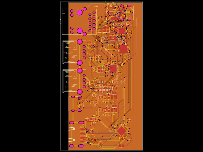 More from this authormohan-bee/hubThis design implements a compact USB-C hub with HDMI output, gigabit Ethernet, multiple USB ports, and integrated power management and ESD protection components.
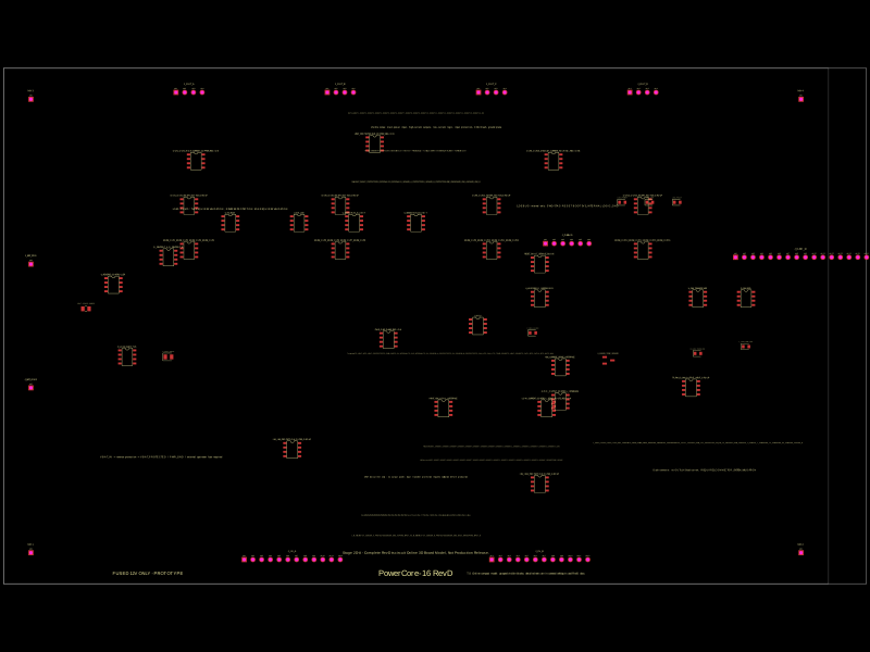 Similar packagejettos/powercore16-revc-complete-board-modelThis code defines the hardware layout for a power distribution and control circuit featuring high-current power inputs, multiple output switches with programmable fuses, MCU-based control, input connectors, and communication interfaces, all represented with specific component footprints and connectivity zones.
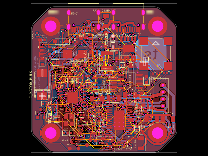 Discover something newimrishabh18/rp2040-motor-controllerA 4-layer RP2040-based NEMA17 stepper-motor controller PCB with USB-C PD power negotiation, DRV8825 dual H-bridge driver, current/temperature sensing, optional encoder, RGB/buzzer status outputs, protection, and programming interfaces.