mohan-bee/gimbal-one-budget-pcb
A 4-layer STM32-based gimbal controller PCB with an onboard LSM6DS3TR-C IMU, three DRV8313 3-phase motor drivers, protected 3S battery input, 3.3 V buck regulation, and SWD/UART control interfaces.
- Version
- 0.1.0
- License
- unset
- Stars
- 0
imports/LSM6DS3TR_C.tsx
import type { ChipProps } from "@tscircuit/props"

const pinLabels = {
  pin1: ["SDO","SA0"],
  pin2: ["SDx"],
  pin3: ["SCx"],
  pin4: ["INT1"],
  pin5: ["VDDIO"],
  pin6: ["GND1"],
  pin7: ["GND2"],
  pin8: ["VDD"],
  pin9: ["INT2"],
  pin10: ["NC1"],
  pin11: ["NC2"],
  pin12: ["CS"],
  pin13: ["SCL"],
  pin14: ["SDA"]
} as const

const pinAttributes = {
  pin5: {requiresPower: true},
  pin6: {requiresGround: true},
  pin7: {requiresGround: true},
  pin8: {requiresPower: true},
  pin10: {doNotConnect: true},
  pin11: {doNotConnect: true}
} as const

export const LSM6DS3TR_C = (props: ChipProps<typeof pinLabels>) => {
  return (
    <chip
      pinLabels={pinLabels}
      pinAttributes={pinAttributes}
      supplierPartNumbers={{
  "jlcpcb": [
    "C967633"
  ]
}}
      manufacturerPartNumber="LSM6DS3TR-C"
      // ST TN0018 rev 8: package land 0.475 x 0.25 + 0.1 mm; 82% paste area.
      footprint={<footprint>
        <keepout allowPlacements shape="rect" pcbX={0} pcbY={0} width={1.8} height={1.3} layers={["top"]} />
        <smtpad solderMaskMargin={0.05} solderPasteMargin={-0.02} portHints={["pin1"]} pcbX="-1.261999mm" pcbY="0.750062mm" width="0.575mm" height="0.35mm" shape="rect" />
<smtpad solderMaskMargin={0.05} solderPasteMargin={-0.02} portHints={["pin2"]} pcbX="-1.261999mm" pcbY="0.249936mm" width="0.575mm" height="0.35mm" shape="rect" />
<smtpad solderMaskMargin={0.05} solderPasteMargin={-0.02} portHints={["pin3"]} pcbX="-1.261999mm" pcbY="-0.249936mm" width="0.575mm" height="0.35mm" shape="rect" />
<smtpad solderMaskMargin={0.05} solderPasteMargin={-0.02} portHints={["pin4"]} pcbX="-1.261999mm" pcbY="-0.750062mm" width="0.575mm" height="0.35mm" shape="rect" />
<smtpad solderMaskMargin={0.05} solderPasteMargin={-0.02} portHints={["pin5"]} pcbX="-0.499999mm" pcbY="-1.012444mm" width="0.35mm" height="0.575mm" shape="rect" />
<smtpad solderMaskMargin={0.05} solderPasteMargin={-0.02} portHints={["pin6"]} pcbX="-0.000127mm" pcbY="-1.012444mm" width="0.35mm" height="0.575mm" shape="rect" />
<smtpad solderMaskMargin={0.05} solderPasteMargin={-0.02} portHints={["pin7"]} pcbX="0.499999mm" pcbY="-1.012444mm" width="0.35mm" height="0.575mm" shape="rect" />
<smtpad solderMaskMargin={0.05} solderPasteMargin={-0.02} portHints={["pin8"]} pcbX="1.261999mm" pcbY="-0.750062mm" width="0.575mm" height="0.35mm" shape="rect" />
<smtpad solderMaskMargin={0.05} solderPasteMargin={-0.02} portHints={["pin9"]} pcbX="1.261999mm" pcbY="-0.249936mm" width="0.575mm" height="0.35mm" shape="rect" />
<smtpad solderMaskMargin={0.05} solderPasteMargin={-0.02} portHints={["pin10"]} pcbX="1.261999mm" pcbY="0.249936mm" width="0.575mm" height="0.35mm" shape="rect" />
<smtpad solderMaskMargin={0.05} solderPasteMargin={-0.02} portHints={["pin11"]} pcbX="1.261999mm" pcbY="0.750062mm" width="0.575mm" height="0.35mm" shape="rect" />
<smtpad solderMaskMargin={0.05} solderPasteMargin={-0.02} portHints={["pin12"]} pcbX="0.499999mm" pcbY="1.012444mm" width="0.35mm" height="0.575mm" shape="rect" />
<smtpad solderMaskMargin={0.05} solderPasteMargin={-0.02} portHints={["pin13"]} pcbX="-0.000127mm" pcbY="1.012444mm" width="0.35mm" height="0.575mm" shape="rect" />
<smtpad solderMaskMargin={0.05} solderPasteMargin={-0.02} portHints={["pin14"]} pcbX="-0.499999mm" pcbY="1.012444mm" width="0.35mm" height="0.575mm" shape="rect" />
<silkscreenpath route={[{"x":0.8303767999999536,"y":1.326210200000105},{"x":1.576069999999845,"y":1.326210200000105},{"x":1.576069999999845,"y":1.0804906000000756}]} />
<silkscreenpath route={[{"x":0.8303767999999536,"y":-1.326210200000105},{"x":1.576069999999845,"y":-1.326210200000105},{"x":1.576069999999845,"y":-1.0804906000000756}]} />
<silkscreenpath route={[{"x":-0.8306307999999945,"y":1.326210200000105},{"x":-1.5763240000001133,"y":1.326210200000105},{"x":-1.5763240000001133,"y":1.0804906000000756}]} />
<silkscreenpath route={[{"x":-0.8306307999999945,"y":-1.326210200000105},{"x":-1.5763240000001133,"y":-1.326210200000105},{"x":-1.5763240000001133,"y":-1.0804906000000756}]} />
<silkscreencircle pcbX="-1.905127mm" pcbY="0.762mm" radius="0.07493mm" />
<silkscreentext text="{NAME}" pcbX="-0.190627mm" pcbY="2.3462mm" anchorAlignment="center" fontSize="1mm" />
<courtyardoutline outline={[{"x":-1.8495015000000876,"y":1.599946500000101},{"x":1.849501499999974,"y":1.599946500000101},{"x":1.849501499999974,"y":-1.5999464999999873},{"x":-1.8495015000000876,"y":-1.5999464999999873},{"x":-1.8495015000000876,"y":1.599946500000101}]} />
      </footprint>}
      cadModel={{
        objUrl: "https://modelcdn.tscircuit.com/easyeda_models/assets/C967633.obj?uuid=f43373e142124ec98babb70d58d97864",
        stepUrl: "https://modelcdn.tscircuit.com/easyeda_models/assets/C967633.step?uuid=f43373e142124ec98babb70d58d97864",
        pcbRotationOffset: 0,
        modelOriginPosition: { x: 0.00012700000002041634, y: -0.000012700000070253736, z: 0 },
      }}
      {...props}
    />
  )
}
Related Packages
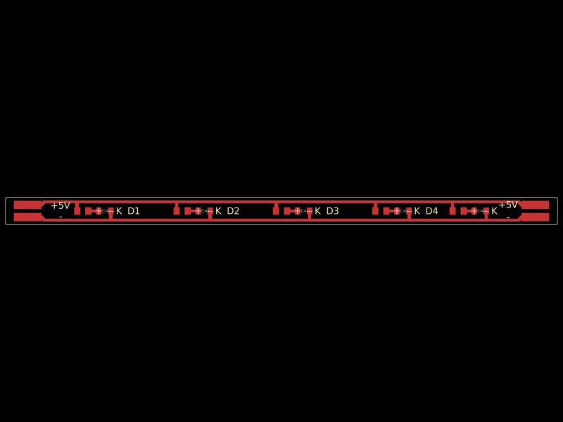 More from this authormohan-bee/warm5-flex-stripA 5 V flexible PCB strip with five parallel warm-white LED branches, each current-limited by a 330 Ω resistor, plus input/output power test terminals and pass-through connections.
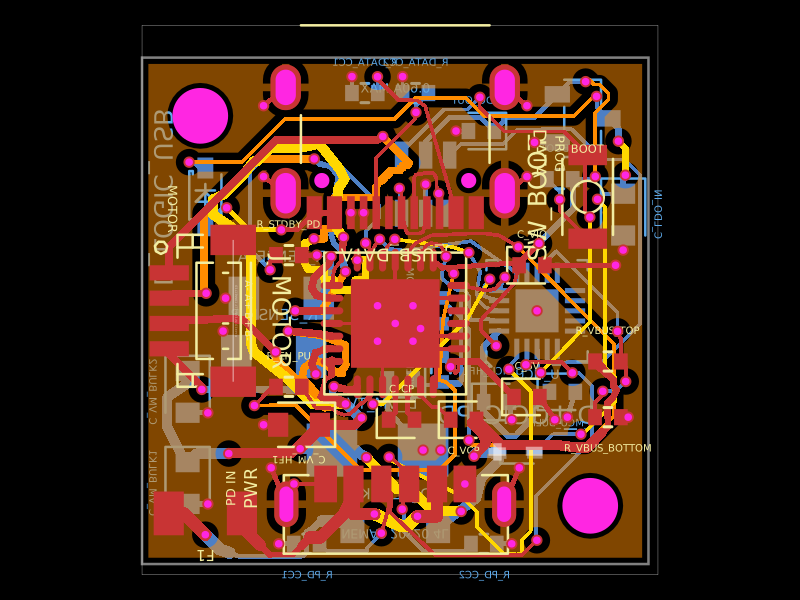 Similar packageShiboSoftwareDev/nema8-20mm-usbc-pd-controllerA 20×20 mm four-layer USB‑C PD stepper motor controller PCB using a CH32X035 MCU, TMC2209 driver, protected power inputs, USB data/boot interface, 3.3 V regulation, ESD/TVS protection, current-sense circuitry, and NEMA‑8 motor outputs.
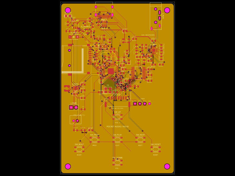 Discover something newDevesh36/pocket-audio-playerA portable, rechargeable microSD audio player built around an RP2040, SPI flash, USB‑C charging/power management, LCD/button controls, PCM5102A I²S DAC, and TPA6132A headphone amplifier in a 3D‑printed enclosure.