mohan-bee/fitness-band-sensor-flex
A flexible dual-sensor PCB integrating a MAX30102 optical PPG/heart-rate sensor and TMP117 digital skin-temperature sensor, with I²C, power regulation, decoupling capacitors, interrupt pull-up, flex-tail connector, test points, and mechanical stiffeners/bend support.
- Version
- 0.0.1
- License
- unset
- Stars
- 0
index.circuit.tsx
PCB
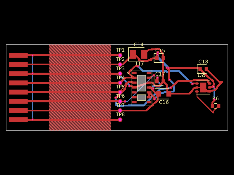
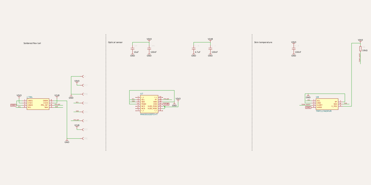
Schematic
import { Fragment } from "react"
import { MAX30102 } from "./imports/MAX30102"
import { TMP117AIDRVR } from "./imports/TMP117AIDRVR"
import { FlexLanding, flexSignals, Rails } from "./interconnect"
import { Cap, Pullup } from "./parts"

export default function SensorFlex() {
  return <board width={36} height={14} material="flex" layers={2} thickness={0.12} autorouter="auto-local" minTraceWidth={0.15} minTraceToPadEdgeClearance={0.15} minPadEdgeToPadEdgeClearance={0.15} minViaPadDiameter={0.45} minViaHoleDiameter={0.2} minBoardEdgeClearance={0.2} pcbStyle={{silkscreenFontSize:0.8,viaPadDiameter:0.45,viaHoleDiameter:0.2}}>
    <Rails />
    <schematicsection name="Link" displayName="Soldered flex tail" />
    <schematicsection name="PPG" displayName="Optical sensor" />
    <schematicsection name="Temperature" displayName="Skin temperature" />
    <FlexLanding name="J_TAIL" pcbX={-16} pcbY={0} schX={-10} schY={0} schSectionName="Link" />
    {flexSignals.map((signal,i)=><Fragment key={String(i)}>
      <testpoint doNotPlace name={`TP${i+1}`} pcbX={0.5} pcbY={5.25-i*1.5} schX={-6} schY={2.5-i*0.8} schSectionName="Link" padDiameter={0.6} connections={{pin1:`net.${signal}`}} />
      <trace name={`TAIL_${i+1}`} from={`.J_TAIL > .pin${i+1}`} to={`.TP${i+1} > .pin1`} width={0.3} pcbPath={[`.J_TAIL > .pin${i+1}`,`.TP${i+1} > .pin1`]} />
    </Fragment>)}
    <trace name="TAIL_GROUND_13" from=".J_TAIL > .pin1" to=".J_TAIL > .pin3" width={0.2} pcbPath={[{x:2.3,y:5.25,via:true,toLayer:"bottom"},{x:2.3,y:3.75},{x:2.3,y:2.25,via:true,toLayer:"top"}]} />
    <trace name="TAIL_GROUND_38" from=".J_TAIL > .pin3" to=".J_TAIL > .pin8" width={0.2} pcbPath={[{x:2.3,y:2.25,via:true,toLayer:"bottom"},{x:2.3,y:-1.5},{x:2.3,y:-5.25,via:true,toLayer:"top"}]} />
    <pcbstiffener name="TAIL_SUPPORT" shape="rect" pcbX={-15} pcbY={0} width={6} height={14} layer="bottom" material="polyimide" thickness={0.15} adhesiveThickness={0.025} />
    <pcbstiffener name="OPTICAL_SUPPORT" shape="rect" pcbX={5} pcbY={0} width={10} height={14} layer="bottom" material="fr4" thickness={0.4} adhesiveThickness={0.025} />
    <pcbstiffener name="TEMP_SUPPORT" shape="rect" pcbX={14.5} pcbY={0} width={7} height={14} layer="bottom" material="fr4" thickness={0.4} adhesiveThickness={0.025} />
    {/* Static 180-degree fold; optical top face turns toward skin below the main board. */}
    <pcbbend name="STATIC_BEND" x1={-6} y1={-7} x2={-6} y2={7} bendAngle={-180} bendRadius={3} bendSide="right" />
    <keepout shape="rect" pcbX={-6} pcbY={0} width={10} height={14} layers={["top","bottom"]} allowTraces />
    <trace name="PPG_SDA_ESCAPE" from=".TP5 > .pin1" to=".U7 > .SDA" width={0.15} pcbPath={[".TP5 > .pin1",{x:1,y:1.5501},".U7 > .SDA"]} />
    <trace name="PPG_INT_BOTTOM_ESCAPE" from=".TP6 > .pin1" to=".U7 > .N_INT" width={0.15} pcbPath={[".TP6 > .pin1",{x:0.8,y:0,via:true,toLayer:"bottom"},{x:1.25,y:0},{x:5.5,y:4.25,via:true,toLayer:"top"},".U7 > .N_INT"]} />
    <MAX30102 name="U7" pcbX={4} pcbY={0} schX={0} schY={0} schSectionName="PPG"
      connections={{SCL:"net.SCL",SDA:"net.SDA",PGND:"net.GND",GND:"net.GND",VLED_POS1:"net.V3V3",VLED_POS2:"net.V3V3",VDD:"net.V1V8",N_INT:"net.PPG_INT"}} />
    <Cap name="C14" capacitance="10uF" pcbX={3.5} pcbY={5.4} schX={-1.5} schY={5} schSectionName="PPG" connections={{pin1:"net.V3V3",pin2:"net.GND"}} />
    <Cap name="C15" capacitance="100nF" pcbX={7} pcbY={4.8} schX={0} schY={5} schSectionName="PPG" connections={{pin1:"net.V3V3",pin2:"net.GND"}} />
    <Cap name="C16" capacitance="4.7uF" pcbX={7.6} pcbY={-1} schX={4} schY={5} schSectionName="PPG" connections={{pin1:"net.V1V8",pin2:"net.GND"}} />
    <Cap name="C17" capacitance="100nF" pcbX={7} pcbY={1} schX={5.5} schY={5} schSectionName="PPG" connections={{pin1:"net.V1V8",pin2:"net.GND"}} />
    <TMP117AIDRVR schWidth={2} name="U8" pcbX={14} pcbY={0} schX={16} schY={0} schSectionName="Temperature"
      connections={{SCL:"net.SCL",SDA:"net.SDA",V_POS:"net.V3V3",GND:"net.GND",EP:"net.GND",ADD0:"net.GND",ALERT:"net.TEMP_ALERT"}} />
    <trace name="TEMP_LOCAL_GROUND" from=".U8 > .pin2" to=".U8 > .pin7" width={0.15} pcbPath={[".U8 > .pin2",".U8 > .pin7"]} />
    <Cap name="C18" capacitance="100nF" pcbX={14} pcbY={3} schX={13} schY={5} schSectionName="Temperature" connections={{pin1:"net.V3V3",pin2:"net.GND"}} />
    <Pullup name="R6" resistance="10k" pcbX={16} pcbY={-3} schX={19} schY={5} schSectionName="Temperature" connections={{pin1:"net.V3V3",pin2:"net.TEMP_ALERT"}} />
  </board>
}