mohan-bee/esp32-c3
This hardware design integrates an ESP32-C3 microcontroller, a USB-C connector, a power management IC (AP2112-3.3V regulator), a USB-to-Serial converter (CH340C), several resistors, capacitors, and user-accessible headers to facilitate USB communication, power regulation, and general I/O interfacing.
- Version
- 1.0.1
- License
- ISC
- Stars
- 0
index.circuit.tsx
PCB
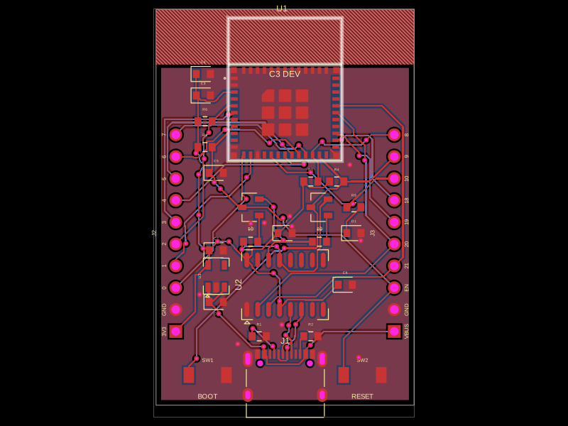
Schematic

import { TYPE_C_16PIN_2MD_073_ } from "./imports/TYPE_C_16PIN_2MD_073_"
import { ESP32_C3_MINI_1_H4X } from './imports/ESP32_C3_MINI_1_H4X'
import { CH340C } from './imports/CH340C'
import { AP2112K_3_3TRG1 } from './imports/AP2112K_3_3TRG1'
import { MMBT3904 } from './imports/MMBT3904'
import { TS_1088_AR02016 } from './imports/TS_1088_AR02016'

const left = ['V3V3','GND','IO0','IO1','IO2','IO3','IO4','IO5','IO6','IO7']
const right = ['VBUS','GND','EN','IO21','IO20','IO19','IO18','IO10','IO9','IO8']
const resistors = [
 ['R1','5.1k',-3,-15,'USB','CC1','GND'],
 ['R2','5.1k',3,-15,'USB','CC2','GND'],
 ['R3','10k',-9.3,7,'MCU','V3V3','EN'],
 ['R4','10k',6,3,'MCU','V3V3','IO9'],
 ['R5','10k',3,3,'MCU','V3V3','IO8'],
 ['R6','10k',-9.3,10,'MCU','V3V3','IO2'],
 ['R7','10k',-4,-4,'AUTO','DTR','BASE_EN'],
 ['R8','10k',4,-4,'AUTO','RTS','BASE_BOOT'],
 ['R9','1k',8,0,'LED','IO10','LED_A'],
] as const
const capacitors = [
 ['C1','10uF',-8,-11,'POWER','VBUS'],
 ['C2','10uF',-8,-5,'POWER','V3V3'],
 ['C3','10uF',-9.5,13,'MCU','V3V3'],
 ['C4','100nF',-9.5,15.5,'MCU','V3V3'],
 ['C5','1uF',-8,4,'MCU','EN'],
 ['C6','100nF',7,-9,'USB','V3V3'],
 ['C7','100nF',0,-3,'USB','V3V3'],
] as const
export default function Board() {
 return <board width={30} height={46} layers={2} thickness={1.6} minViaHoleDiameter={0.3} minViaPadDiameter={0.6} autorouter="auto_local" minTraceWidth={0.18} schAutoLayoutEnabled>
  {['USB','POWER','MCU','AUTO','LED','HEADERS'].map(name=><schematicsection key={name} name={name} />)}
  {['VBUS','V3V3','GND','CC1','CC2','USB_DP','USB_DM','DTR','RTS','EN','BASE_EN','BASE_BOOT','LED_A',...Array.from({length:11},(_,i)=>`IO${i}`),'IO18','IO19','IO20','IO21'].map(name=><net key={name} name={name} />)}
  <TYPE_C_16PIN_2MD_073_ name="J1" schWidth={1.2} schPinArrangement={{rightSide:{pins:[16,25,18,24,20,22,21,19,23,17,15,26,13,14,27,28],direction:"top-to-bottom"}}} pcbX={0} pcbY={-19.2} pcbRotation={0} schSectionName="USB" connections={{VBUS1:'net.VBUS',VBUS2:'net.VBUS',GND1:'net.GND',GND2:'net.GND',SHELL1:'net.GND',SHELL2:'net.GND',SHELL3:'net.GND',SHELL4:'net.GND',CC1:'net.CC1',CC2:'net.CC2',DP1:'net.USB_DP',DP2:'net.USB_DP',DM1:'net.USB_DM',DM2:'net.USB_DM'}} />
  <CH340C name="U2" pcbX={0} pcbY={-9} schSectionName="USB" connections={{GND:'net.GND',VCC:'net.V3V3',V3:'net.V3V3',D_POS:'net.USB_DP',D_NEG:'net.USB_DM',TXD:'net.IO20',RXD:'net.IO21',N_DTR:'net.DTR',N_RTS:'net.RTS'}} />
  <AP2112K_3_3TRG1 name="U3" schHeight={0.6} pcbX={-8} pcbY={-8} schSectionName="POWER" connections={{VIN:'net.VBUS',EN:'net.VBUS',GND:'net.GND',VOUT:'net.V3V3'}} />
  <ESP32_C3_MINI_1_H4X name="U1" schHeight={6.2} pcbX={0} pcbY={11} schSectionName="MCU" connections={{'3V3':'net.V3V3',EN:'net.EN',RXD0:'net.IO20',TXD0:'net.IO21',...Object.fromEntries([...Array.from({length:11},(_,i)=>i),18,19].map(i=>[`IO${i}`,`net.IO${i}`])),...Object.fromEntries(Array.from({length:30},(_,i)=>[`GND${i+1}`,'net.GND']))}} />
  <MMBT3904 name="Q1" schHeight={0.4} pcbX={-4} pcbY={0} schSectionName="AUTO" connections={{B:'net.BASE_EN',E:'net.RTS',C:'net.EN'}} />
  <MMBT3904 name="Q2" schHeight={0.4} pcbX={4} pcbY={0} schSectionName="AUTO" connections={{B:'net.BASE_BOOT',E:'net.DTR',C:'net.IO9'}} />
  <TS_1088_AR02016 name="SW1" pcbX={-9} pcbY={-19.5} schSectionName="AUTO" connections={{pin1:'net.IO9',pin2:'net.GND'}} />
  <TS_1088_AR02016 name="SW2" pcbX={9} pcbY={-19.5} schSectionName="AUTO" connections={{pin1:'net.EN',pin2:'net.GND'}} />
  <led name="D1" color="green" footprint="0603" pcbX={8} pcbY={-3} schSectionName="LED" connections={{anode:'net.LED_A',cathode:'net.GND'}} />
  {resistors.map(([name,resistance,pcbX,pcbY,section,a,b])=><resistor key={name} name={name} resistance={resistance} footprint="0603" pcbX={pcbX} pcbY={pcbY} schSectionName={section} connections={{pin1:`net.${a}`,pin2:`net.${b}`}} />)}
  {capacitors.map(([name,capacitance,pcbX,pcbY,section,a])=><capacitor key={name} schOrientation="vertical" name={name} capacitance={capacitance} voltageRating={10} footprint="0603" pcbX={pcbX} pcbY={pcbY} schSectionName={section} connections={{pin1:`net.${a}`,pin2:'net.GND'}} />)}
  {[left,right].map((nets,i)=><pinheader key={i} name={`J${i+2}`} pinCount={10} pitch={2.54} pcbRotation={90} pcbX={i===0?-12.7:12.7} pcbY={-3} schSectionName="HEADERS" pcbPinLabels={Object.fromEntries(nets.map((n,j)=>[`pin${j+1}`,n]))} connections={Object.fromEntries(nets.map((n,j)=>[`pin${j+1}`,`net.${n}`]))} />)}
  <keepout shape="rect" pcbX={0} pcbY={19.8} width={30} height={6.4} layers={['top','bottom']} />
  {['top','bottom'].map(layer=><copperpour key={layer} name={`GND_${layer}`} layer={layer as 'top'|'bottom'} connectsTo="net.GND" clearance={0.2} boardEdgeMargin={0.3} outline={[{x:-14.7,y:-22.7},{x:14.7,y:-22.7},{x:14.7,y:16.5},{x:-14.7,y:16.5}]} />)}
  {[left,right].map((nets,i)=>nets.map((n,j)=><silkscreentext key={`label-${i}-${j}`} text={n.replace("V3V3","3V3").replace("IO","")} pcbX={i===0?-14.1:14.1} pcbY={-14.43+j*2.54} pcbRotation={90} fontSize={0.65} />))}
  <silkscreentext text="C3 DEV" pcbX={0} pcbY={15.5} fontSize={1} />
  <silkscreentext text="BOOT" pcbX={-9} pcbY={-22} fontSize={0.8} />
  <silkscreentext text="RESET" pcbX={9} pcbY={-22} fontSize={0.8} />
 </board>
}