imrishabh18/rp2040-motor-controller
An RP2040-based NEMA17 stepper-motor controller with USB-C programming and PD motor-power negotiation, DRV8825 dual H-bridge drive, current/temperature telemetry, protected power filtering, status RGB LED, buzzer alarm, and optional magnetic encoder.
- Version
- 1.0.41
- License
- unset
- Stars
- 3
scripts/audit-driver-thermal-vias.py
"""Check the DRV8825 heat path and the actual exported drill/mask geometry.

Uses Shapely (the same environment as audit-manufacturing.py). The small Gerber
reader deliberately rejects unsupported drawing commands instead of assuming
an unrecognized mask operation is harmless.
"""
import hashlib
import json
import re
import zipfile
from pathlib import Path
from shapely.geometry import Point, LineString, Polygon, box
from shapely.affinity import translate, rotate
from shapely.ops import unary_union


from gerber_geometry import gerber_geometry


root = Path(__file__).resolve().parents[1]
circuit_path = root / 'dist/index/circuit.json'
archive = root / 'dist/index/gerbers.zip'
j = json.loads(circuit_path.read_text())
sha = hashlib.sha256(circuit_path.read_bytes()).hexdigest()
manufacturing = json.loads((root / 'reports/manufacturing-audit.json').read_text())
assert manufacturing['sha256'] == sha, 'Run the complete manufacturing audit first'
for field in ('unmappedElements', 'shortContacts', 'splitNets', 'holeSpacingViolations', 'holeToCopperViolations', 'pthDrillToCopperViolations', 'npthToCopperViolations', 'copperToBoardEdgeViolations'):
    assert not manufacturing[field], f'Manufacturing audit failed: {field}'
driver = next(e for e in j if e['type'] == 'source_component' and e['name'] == 'DRIVER')
pc = next(e for e in j if e['type'] == 'pcb_component' and e['source_component_id'] == driver['source_component_id'])
ep = next(e for e in j if e['type'] == 'pcb_smtpad' and e.get('pcb_component_id') == pc['pcb_component_id'] and 'pin29' in e.get('port_hints', []))
land = box(ep['x']-ep['width']/2, ep['y']-ep['height']/2, ep['x']+ep['width']/2, ep['y']+ep['height']/2)
land = rotate(land, ep.get('ccw_rotation', 0), origin=(ep['x'], ep['y']))
ground = next(e['source_net_id'] for e in j if e['type'] == 'source_net' and e['name'] == 'GND')
joins = [e for e in j if e['type'] == 'source_trace' and re.fullmatch(r'DRV_IMPORTED_EP_\d+ connectivity', e.get('display_name', ''))]
assert len(joins) == 12
vias = []
for join in joins:
    assert ep['pcb_port_id'] in {e['pcb_port_id'] for e in j if e['type'] == 'pcb_port' and e.get('source_port_id') in join['connected_source_port_ids']}
    matching = [e for e in j if e['type'] == 'pcb_via' and e.get('source_trace_id') == join['source_trace_id']]
    assert len(matching) == 1
    vias.extend(matching)
assert len({(v['x'], v['y']) for v in vias}) == 12
pours = {}
for layer in ('inner1', 'inner2', 'bottom'):
    shapes = []
    for e in j:
        if e['type'] != 'pcb_copper_pour' or e['layer'] != layer or e['source_net_id'] != ground:
            continue
        b = e['brep_shape']; xy = lambda r: [(v['x'], v['y']) for v in r['vertices']]
        shapes.append(Polygon(xy(b['outer_ring']), [xy(r) for r in b['inner_rings']]))
    pours[layer] = unary_union(shapes)

with zipfile.ZipFile(archive) as z:
    top_mask = gerber_geometry(z.read('F_Mask.gbr').decode())
    bottom_mask = gerber_geometry(z.read('B_Mask.gbr').decode())
    drill_text = z.read('drill-L1-L4.drl').decode()
    assert 'FileFunction,Plated,1,4,PTH' in drill_text
    sizes = {int(n): float(d) for n, d in re.findall(r'^T(\d+)C([\d.]+)#39;, drill_text, re.M)}
    tool = None; drills = []
    for line in drill_text.splitlines():
        if re.fullmatch(r'T\d+', line): tool = int(line[1:])
        m = re.fullmatch(r'X(-?[\d.]+)Y(-?[\d.]+)', line)
        if m: drills.append((float(m[1]), float(m[2]), sizes[tool]))

details = []
for via in vias:
    x, y = via['x'], via['y']; center = Point(x, y)
    assert abs(via['hole_diameter'] - 0.3000248) < 1e-8 and abs(via['outer_diameter'] - 0.5000244) < 1e-8
    assert set(via['layers']) == {'top', 'inner1', 'inner2', 'bottom'}
    assert land.covers(center.buffer(via['outer_diameter']/2)), 'Via ring leaves exposed pad'
    # Require the full circumference of the ring embedded in ground copper,
    # not only a spoke connection (TI PowerPAD SLMA004B, Figure 3).
    for layer, copper in pours.items():
        assert copper.buffer(1e-7).covers(center.buffer(via['outer_diameter']/2)), f'No solid {layer} pour around {via["pcb_via_id"]}'
    assert top_mask.buffer(1e-7).covers(center.buffer(via['outer_diameter']/2)), 'Top thermal solder land was masked'
    mask_clearance = center.distance(bottom_mask) - via['outer_diameter']/2
    assert mask_clearance >= 0.1, 'Bottom solder-mask opening exposes a thermal via'
    # Excellon coordinates are rounded to four decimal places in millimetres.
    assert sum(abs(dx-x) <= 0.00005001 and abs(dy-y) <= 0.00005001 and abs(d-via['hole_diameter']) < 1e-5 for dx, dy, d in drills) == 1
    details.append({'x': x, 'y': y, 'drillMm': via['hole_diameter'], 'padMm': via['outer_diameter'], 'bottomMaskOpeningClearanceMm': mask_clearance})
result = {
    'status': 'pass', 'circuitJsonSha256': sha,
    'gerbersSha256': hashlib.sha256(archive.read_bytes()).hexdigest(),
    'inPadThermalViaCount': len(vias), 'manuallyAddedThermalViaCount': 0, 'supplierPart': 'C81582',
    'solidGroundContactLayers': ['top thermal pad', 'inner1', 'inner2', 'bottom'],
    'topThermalPadSolderable': True, 'bottomThermalViasTentedInGerber': True,
    'platedThroughDrillsVerified': True, 'vias': details,
}
(root / 'reports/driver-thermal-vias.json').write_text(json.dumps(result, indent=2)+'\n')
print(json.dumps(result, indent=2))
Related Packages
 More from this authorimrishabh18/3d-model-testIt loads a 3D model of an electronic component onto a circuit board with specified positioning.
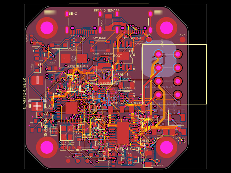 Similar packageastra/nema17-stepper-motor-controller-spring-clamp-rp2040A 4-layer RP2040 controller board that negotiates USB‑C PD motor power and drives a NEMA17 stepper via a DRV8825, with current sensing, thermal shutdown, RGB status LED, buzzer alarm, optional AS5600 encoder, protection/filtering, and test points.
 Discover something newseveibar/am3352-dev-board-4layer-dogboneDefines PCB footprints and pin mappings for a TI AM3352ZCZ100 processor, JST GH connectors, and assembly-part lookup helpers for capacitors, resistors, and headers.