imrishabh18/rp2040-motor-controller
An RP2040-based NEMA17 stepper-motor controller with USB-C programming and PD motor-power negotiation, DRV8825 dual H-bridge drive, current/temperature telemetry, protected power filtering, status RGB LED, buzzer alarm, and optional magnetic encoder.
- Version
- 1.0.41
- License
- unset
- Stars
- 3
schematic/MotorDriverCoreSection.tsx
import { Drv8825Support } from "./Drv8825Support";
import { revisionPlacement } from "../mechanical/revision-placement";
import { HoLRT1206_1W_300mR_1_ } from "../imports/HoLRT1206_1W_300mR_1_";
import { DRV8825PWPR } from "../imports/DRV8825PWPR";
import { BSS84 } from "../imports/BSS84";
import { Fragment } from "react";
import {
	groundTrace,
	logicTrace,
	powerTrace,
	schematicSections,
	schematicSheets,
} from "./config";

export const MotorDriverController = () => (
	<>
		<DRV8825PWPR
			name="DRIVER" schWidth={2.2} schHeight={3.8}
      noConnect={["DECAY", "NC", "nHOME"]}
			schX={-5.5}
			schY={0}
			schMarginLeft={1}
			schMarginRight={1}
			schPinArrangement={{
				leftSide: {
					pins: [5, 6, 7, 10, 9, 8, 1, 2, 3],
					direction: "top-to-bottom",
				},
				rightSide: {
					pins: [22, 20, 16, 21, 17, 18, 24, 25, 26, 19, 27, 23],
					direction: "top-to-bottom",
				},
				topSide: {
					pins: [4, 11, 15, 12, 13],
					direction: "left-to-right",
				},
				bottomSide: {
					pins: [14, 28, 29],
					direction: "left-to-right",
				},
			}}
			schPinStyle={{
        ...Object.fromEntries([20,16,21,17,18,24,25,26,19,27,23].map(pin => [`pin${pin}`, {marginTop:0.04}])),
        pin11: {marginLeft:0.1}, pin15: {marginLeft:0.1},
        pin28: {marginLeft:0.3}, pin29: {marginLeft:0.3},
				pin5: {marginTop:0.15},
        pin7: { marginTop: 0.45 },
				pin9: { marginTop: 0.45 },
				pin1: { marginTop: 0.45 },
			}}
			schSheetName={schematicSheets.motorDriver}
			schSectionName={schematicSections.driverCore} {...revisionPlacement("DRIVER", {x:-5.625,y:-8.25})}
		/>
	</>
);

export const MotorDriverPassives = () => (
	<>
    <Drv8825Support />
		<capacitor
			name="C_VM_BULK"
			capacitance="10uF"
      maxVoltageRating="50V"
			footprint="1206"
			supplierPartNumbers={{ jlcpcb: ["C13585"] }}
			manufacturerPartNumber="CL31A106KBHNNNE"
			maxDecouplingTraceLength={7.5}
			schX={-2.5}
			schY={-6}
			schMarginX={0.15}
			schMarginY={0.25}
			schOrientation="vertical"
			schSheetName={schematicSheets.motorDriver}
			schSectionName={schematicSections.driverCore} {...revisionPlacement("C_VM_BULK", {x:-5.625,y:-8.25})}
		/>
		<capacitor
			name="C_VM_HF" maxVoltageRating="50V"
			capacitance="100nF"
			footprint="0402"
			supplierPartNumbers={{ jlcpcb: ["C960916"] }}
			maxDecouplingTraceLength={5.5}
			schX={-1.9}
			schY={-4}
			schMarginX={0.15}
			schMarginY={0.25}
			schOrientation="vertical"
			schSheetName={schematicSheets.motorDriver}
			schSectionName={schematicSections.driverCore} {...revisionPlacement("C_VM_HF", {x:-5.625,y:-8.25})}
		/>
		<HoLRT1206_1W_300mR_1_
			name="R_ISEN_A" schRotation={-90.0}
			schX={-12}
			schY={0.025}
			schSheetName={schematicSheets.motorDriver}
			schSectionName={schematicSections.driverCore} {...revisionPlacement("R_ISEN_A", {x:-5.625,y:-8.25})}
		/>
		<HoLRT1206_1W_300mR_1_
			name="R_ISEN_B" schRotation={-90.0}
			schX={-9}
			schY={-0.825}
			schSheetName={schematicSheets.motorDriver}
			schSectionName={schematicSections.driverCore} {...revisionPlacement("R_ISEN_B", {x:-5.625,y:-8.25})}
		/>
		<resistor
			name="R_SLEEP_PD" schRotation={-90.0}
			resistance="100k"
			footprint="0402"
			supplierPartNumbers={{ jlcpcb: ["C25741"] }}
			schX={-4.25}
			schY={-4.5}
			schSheetName={schematicSheets.motorDriver}
			schSectionName={schematicSections.driverCore} {...revisionPlacement("R_SLEEP_PD", {x:-5.625,y:-8.25})}
		/>
		<resistor
			name="R_FAULT_PU" schRotation={90.0}
			resistance="10k"
			footprint="0402"
			supplierPartNumbers={{ jlcpcb: ["C25744"] }}
			manufacturerPartNumber="0402WGF1002TCE"
			schX={-8}
			schY={-7}
			schSheetName={schematicSheets.motorDriver}
			schSectionName={schematicSections.driverCore} {...revisionPlacement("R_FAULT_PU", {x:-5.625,y:-8.25})}
		/>
		<BSS84
			name="Q_PD_ENABLE"
			schX={-12}
			schY={-3}
			schPinStyle={{ pin3: { marginTop: 0.2 } }}
			schPinArrangement={{
				leftSide: { pins: [1], direction: "top-to-bottom" },
				rightSide: { pins: [2, 3], direction: "top-to-bottom" },
			}}
			schSheetName={schematicSheets.motorDriver}
			schSectionName={schematicSections.driverCore} {...revisionPlacement("Q_PD_ENABLE", {x:-5.625,y:-8.25})}
		/>
		<resistor
			name="R_PD_ENABLE_PU"
			resistance="100k"
			footprint="0402"
			supplierPartNumbers={{ jlcpcb: ["C25741"] }}
			schX={-10.5}
			schY={-5.5}
			schOrientation="vertical"
			schSheetName={schematicSheets.motorDriver}
			schSectionName={schematicSections.driverCore} {...revisionPlacement("R_PD_ENABLE_PU", {x:-5.625,y:-8.25})}
		/>
	</>
);

export const MotorDriverControlTraces = () => (
	<>
		{/* Staggered escape vias keep the 0.4 mm-pitch GPIO fanout outside the QFN. */}
		{[
			{ gpio: 18, x: 0.8250000000000002, y: 0.3493500000000001 },
			{ gpio: 19, x: 1.5750000000000002, y: 0.79945 },
			{ gpio: 20, x: 0.8250000000000002, y: 1.24955 },
		].map(({ gpio, x, y }) => (
			<Fragment key={gpio}>
				<via name={`MCU_GPIO${gpio}_ESCAPE`} pcbX={x} pcbY={y}
					holeDiameter="0.3mm" outerDiameter="0.45mm"
					fromLayer="top" toLayer="bottom"
					connectsTo={[`.MCU > .U1 > .GPIO${gpio}`, `.MCU_GPIO${gpio}_ESCAPE > .top`, `.MCU_GPIO${gpio}_ESCAPE > .bottom`]} />
				<trace name={`MCU_GPIO${gpio}_ESCAPE_TRACE`}
					schDisplayLabel={({18: "DRIVER_STEP", 19: "DRIVER_DIR", 20: "DRIVER_RESET"} as Record<number, string>)[gpio]}
					from={`.MCU > .U1 > .GPIO${gpio}`} to={`.MCU_GPIO${gpio}_ESCAPE > .top`}
					thickness="0.15mm" pcbPath={[`.MCU_GPIO${gpio}_ESCAPE > .top`]} />
			</Fragment>
		))}
		<trace
			name="DRIVER_STEP"
			from=".MCU_GPIO18_ESCAPE > .bottom"
			to=".DRIVER > .STEP"
			{...logicTrace}
		/>
		<trace
			name="DRIVER_DIR"
			from=".MCU_GPIO19_ESCAPE > .bottom"
			to=".DRIVER > .DIR"
			{...logicTrace}
		/>
		<trace
			name="DRIVER_RESET"
			from=".MCU_GPIO20_ESCAPE > .bottom"
			to=".DRIVER > .nRESET"
			{...logicTrace}
		/>
		<trace
			name="DRIVER_ENABLE_N"
			from=".MCU > .U1 > .GPIO21"
			to=".DRIVER > .nENBL"
			{...logicTrace}
		/>
		<trace
			name="DRIVER_SLEEP"
			schDisplayLabel="MCU_ENABLE"
			from=".MCU > .U1 > .GPIO22"
			to=".Q_PD_ENABLE > .source"
			{...logicTrace}
		/>
		<trace
			name="DRIVER_FAULT"
			// Reserve the complete MCU/pull-up/driver fault route before power routing.
			from=".MCU > .U1 > .GPIO23"
			to=".DRIVER > .nFault"
			thickness="0.1mm"
		/>
	</>
);

export const MotorDriverPowerTraces = () => (
	<>
		<trace
			name="VM_BULK"
			from=".DRIVER > .VM"
			to=".C_VM_BULK > .pin1"
			schDisplayLabel="VMOTOR"
			{...powerTrace}
		/>
		<trace
			name="VM_HF"
			from=".DRIVER > .VMB"
			to=".C_VM_HF > .pin1"
			{...powerTrace}
		/>
	</>
);

export const MotorDriverPrimaryGroundTraces = () => (
	<>
		{/* Join the board's scoped GND (pours and sense returns) to the
		    MCU/driver/USB ground network. Matching net names do not join them. */}
		<trace
			name="BOARD_GND_JOIN"
			from=".DRIVER > .EP"
			to="net.GND"
			{...powerTrace}
		/>
		<trace
			name="COMMON_GND"
			from=".DRIVER > .EP"
			to=".MCU > .U1 > .GND"
			{...groundTrace}
		/>
		<trace
			name="DRIVER_GND_JOIN"
			from=".DRIVER > .GND1"
			to=".DRIVER > .EP"
			{...groundTrace}
		/>
	</>
);

export const MotorDriverGroundTraces = () => (
	<>
		<trace
			name="ISEN_A_GND"
			from=".R_ISEN_A > .pin2"
			to="net.GND"
			{...groundTrace}
		/>
		<trace
			name="ISEN_B_GND"
			from=".R_ISEN_B > .pin2"
			to="net.GND"
			{...groundTrace}
		/>
		<trace
			name="VM_BULK_GND"
			from=".C_VM_BULK > .pin2"
			to="net.GND"
			{...groundTrace}
		/>
		<trace
			name="VM_HF_GND"
			from=".C_VM_HF > .pin2"
			to="net.GND"
			{...groundTrace}
		/>
		<trace
			name="SLEEP_PULLDOWN_GND"
			from=".R_SLEEP_PD > .pin2"
			to="net.GND"
			{...logicTrace}
		/>
	</>
);

export const MotorDriverSenseAndControlTraces = () => (
	<>

		<trace
			name="ISEN_A"
			from=".DRIVER > .AISEN"
			to=".R_ISEN_A > .pin1"
			schDisplayLabel="A_ISEN"
			{...powerTrace}
		/>
		<trace
			name="ISEN_B"
			from=".DRIVER > .BISEN"
			to=".R_ISEN_B > .pin1"
			schDisplayLabel="B_ISEN"
			{...powerTrace}
		/>
		<trace
			name="PD_ENABLE_OUTPUT"
			schDisplayLabel="PD_MCU_ENABLE"
			from=".Q_PD_ENABLE > .drain"
			to=".DRIVER > .nSleep"
			{...logicTrace}
		/>
		<trace
			name="PD_ENABLE_GATE"
			from=".Q_PD_ENABLE > .gate"
			to=".U_PD > .PG"
			schDisplayLabel="PD_GOOD"
			{...logicTrace}
		/>
		<trace
			name="PD_ENABLE_GATE_PULLUP"
			from=".R_PD_ENABLE_PU > .pin1"
			to=".Q_PD_ENABLE > .gate"
			{...logicTrace}
		/>
		<trace
			name="PD_ENABLE_PULLUP_SUPPLY"
			from=".R_PD_ENABLE_PU > .pin2"
			to=".U_PD > .VDD"
			{...logicTrace}
		/>
		<trace
			name="SLEEP_PULLDOWN"
			from=".R_SLEEP_PD > .pin1"
			to=".DRIVER > .nSleep"
			schDisplayLabel="nSLEEP"
			{...logicTrace}
		/>
		<trace
			name="FAULT_PULLUP"
			from=".R_FAULT_PU > .pin1"
			to=".DRIVER > .nFault"
			schDisplayLabel="nFAULT"
			thickness="0.1mm"
		/>
		<trace
			name="FAULT_PULLUP_3V3"
			from=".R_FAULT_PU > .pin2"
			to=".MCU > .L_AVDD > .pin1"
			schDisplayLabel="V3V3"
			{...logicTrace}
		/>
	</>
);
Related Packages
 More from this authorimrishabh18/3d-model-testIt loads a 3D model of an electronic component onto a circuit board with specified positioning.
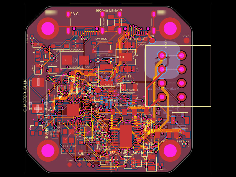 Similar packageastra/nema17-stepper-motor-controller-spring-clamp-rp2040A 4-layer RP2040 controller board that negotiates USB‑C PD motor power and drives a NEMA17 stepper via a DRV8825, with current sensing, thermal shutdown, RGB status LED, buzzer alarm, optional AS5600 encoder, protection/filtering, and test points.
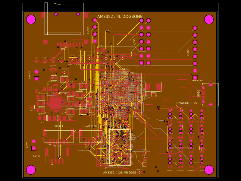 Discover something newseveibar/am3352-dev-board-4layer-dogboneDefines PCB footprints and pin mappings for a TI AM3352ZCZ100 processor, JST GH connectors, and assembly-part lookup helpers for capacitors, resistors, and headers.