imrishabh18/rp2040-motor-controller
The circuit implements a powered USB interface with a W25Q16 flash memory chip, a RP2040 microcontroller, and AO3400A MOSFETs for switch control, enabling USB communication, memory storage, and device power management.
- Version
- 1.0.19
- License
- unset
- Stars
- 0
reports/encoder-bottom-schematic-placement.log
Detected entrypoint: 'index.circuit.tsx'
trace: `key` is not a prop. Trying to access it will result in `undefined` being returned. If you need to access the same value within the child component, you should pass it as a different prop. (https://react.dev/link/special-props)
<SchematicSheet name="position_alarm" id="schematic_sheet_5">
<SchematicBoxPositions>
<SchematicBoxPlacement componentName="U_ENCODER" positionAnchor="center" schX="-5" schY="2" width="1.8" height="1.6" />
<SchematicBoxPlacement componentName="R_ENC_SDA" positionAnchor="center" schX="-11" schY="2.2" width="0.9" height="0.6" />
<SchematicBoxPlacement componentName="Q_BUZZER" positionAnchor="center" schX="5" schY="0" width="1.2" height="0.8" />
</SchematicBoxPositions>
<SchematicPlacementIssues>
<GenericSchematicBoxTooWide message="Shrink schematic box width" componentName="U_ENCODER" currentSchWidth="1.8" measuredInnerLabelHorizontalEmptySpace="1.03" maxAllowedInnerLabelHorizontalEmptySpace="1" suggestedSchWidth="1.77" />
<SchematicPinPaddingToEdgeTooLarge message="Move schematic pins closer to the box edge or change the schematic box width" componentName="U_ENCODER" pinSide="top" edgeSide="left" pinName="VDD5V" measuredPadding="0.8" maxAllowedPadding="0.385" excessPadding="0.415" suggestedSchWidth="0.97" />
<SchematicPinPaddingToEdgeTooLarge message="Move schematic pins closer to the box edge or change the schematic box width" componentName="U_ENCODER" pinSide="top" edgeSide="right" pinName="VDD3V3" measuredPadding="0.8" maxAllowedPadding="0.385" excessPadding="0.415" suggestedSchWidth="0.97" />
<SchematicPinPaddingToEdgeTooLarge message="Move schematic pins closer to the box edge or change the schematic box height" componentName="U_ENCODER" pinSide="right" edgeSide="top" pinName="OUT" measuredPadding="0.7" maxAllowedPadding="0.528" excessPadding="0.172" suggestedSchHeight="1.255" />
<SchematicPinPaddingToEdgeTooLarge message="Move schematic pins closer to the box edge or change the schematic box height" componentName="U_ENCODER" pinSide="right" edgeSide="bottom" pinName="PGO" measuredPadding="0.7" maxAllowedPadding="0.528" excessPadding="0.172" suggestedSchHeight="1.255" />
<SchematicPinPaddingToEdgeTooLarge message="Move schematic pins closer to the box edge or change the schematic box width" componentName="U_ENCODER" pinSide="bottom" edgeSide="left" pinName="GND" measuredPadding="0.8" maxAllowedPadding="0.385" excessPadding="0.415" suggestedSchWidth="0.97" />
<SchematicPinPaddingToEdgeTooLarge message="Move schematic pins closer to the box edge or change the schematic box width" componentName="U_ENCODER" pinSide="bottom" edgeSide="right" pinName="DIR" measuredPadding="0.8" maxAllowedPadding="0.385" excessPadding="0.415" suggestedSchWidth="0.97" />
<SchematicPinPaddingToEdgeTooLarge message="Move schematic pins closer to the box edge or change the schematic box height" componentName="U_ENCODER" pinSide="left" edgeSide="top" pinName="SDA" measuredPadding="0.7" maxAllowedPadding="0.528" excessPadding="0.172" suggestedSchHeight="1.255" />
<SchematicPinPaddingToEdgeTooLarge message="Move schematic pins closer to the box edge or change the schematic box height" componentName="U_ENCODER" pinSide="left" edgeSide="bottom" pinName="SCL" measuredPadding="0.7" maxAllowedPadding="0.528" excessPadding="0.172" suggestedSchHeight="1.255" />
<SchematicPinPaddingToEdgeTooLarge message="Move schematic pins closer to the box edge or change the schematic box height" componentName="Q_BUZZER" pinSide="left" edgeSide="top" pinName="G" measuredPadding="0.3" maxAllowedPadding="0.2" excessPadding="0.1" suggestedSchHeight="0.6" />
<SchematicPinPaddingToEdgeTooLarge message="Move schematic pins closer to the box edge or change the schematic box height" componentName="Q_BUZZER" pinSide="left" edgeSide="bottom" pinName="S" measuredPadding="0.3" maxAllowedPadding="0.2" excessPadding="0.1" suggestedSchHeight="0.6" />
<SchematicPinPaddingToEdgeTooLarge message="Move schematic pins closer to the box edge or change the schematic box height" componentName="Q_BUZZER" pinSide="right" edgeSide="top" pinName="D" measuredPadding="0.4" maxAllowedPadding="0.2" excessPadding="0.2" suggestedSchHeight="0.4" />
<SchematicPinPaddingToEdgeTooLarge message="Move schematic pins closer to the box edge or change the schematic box height" componentName="Q_BUZZER" pinSide="right" edgeSide="bottom" pinName="D" measuredPadding="0.4" maxAllowedPadding="0.2" excessPadding="0.2" suggestedSchHeight="0.4" />
<TraceCanBeSimplifiedByMovingComponent schematicTraceId="schematic_trace_141" targetComponentName="U_ENCODER" deltaSchX="0" deltaSchY="-1.561" newSchX="-5" newSchY="0.439" currentTurnCount="3" suggestedTurnCount="1" message="move U_ENCODER down by 1.561 (to schX=-5, schY=0.439) to reduce this trace from 3 turns to 1" />
</SchematicPlacementIssues>
</SchematicSheet>
<SchematicSheet name="controller_programming" id="schematic_sheet_1">
<SchematicBoxPositions>
<SchematicBoxPlacement componentName="J_USB" positionAnchor="center" schX="2" schY="0.5" width="2.2" height="3.56" />
<SchematicBoxPlacement componentName="U2" positionAnchor="center" schX="10" schY="0.2" width="1.2" height="2.8" />
<SchematicBoxPlacement componentName="U3" positionAnchor="center" schX="-6" schY="0" width="1.2" height="0.95" />
</SchematicBoxPositions>
<SchematicPlacementIssues>
<SchematicPinPaddingToEdgeTooLarge message="Move schematic pins closer to the box edge or change the schematic box height" componentName="J_USB" pinSide="right" edgeSide="top" pinName="EH2" measuredPadding="0.23" maxAllowedPadding="0.2" excessPadding="0.03" suggestedSchHeight="3.5" />
<SchematicPinPaddingToEdgeTooLarge message="Move schematic pins closer to the box edge or change the schematic box height" componentName="J_USB" pinSide="right" edgeSide="bottom" pinName="B8" measuredPadding="0.23" maxAllowedPadding="0.2" excessPadding="0.03" suggestedSchHeight="3.5" />
<SchematicPinPaddingToEdgeTooLarge message="Move schematic pins closer to the box edge or change the schematic box width" componentName="U2" pinSide="bottom" edgeSide="left" pinName="GND" measuredPadding="0.325" maxAllowedPadding="0.2" excessPadding="0.125" suggestedSchWidth="0.95" />
<SchematicPinPaddingToEdgeTooLarge message="Move schematic pins closer to the box edge or change the schematic box width" componentName="U2" pinSide="bottom" edgeSide="right" pinName="EP" measuredPadding="0.325" maxAllowedPadding="0.2" excessPadding="0.125" suggestedSchWidth="0.95" />
<SchematicPinPaddingToEdgeTooLarge message="Move schematic pins closer to the box edge or change the schematic box width" componentName="U2" pinSide="top" edgeSide="left" pinName="VCC" measuredPadding="0.6" maxAllowedPadding="0.2" excessPadding="0.4" suggestedSchWidth="0.4" />
<SchematicPinPaddingToEdgeTooLarge message="Move schematic pins closer to the box edge or change the schematic box width" componentName="U2" pinSide="top" edgeSide="right" pinName="VCC" measuredPadding="0.6" maxAllowedPadding="0.2" excessPadding="0.4" suggestedSchWidth="0.4" />
<SchematicPinPaddingToEdgeTooLarge message="Move schematic pins closer to the box edge or change the schematic box width" componentName="U3" pinSide="bottom" edgeSide="left" pinName="GND" measuredPadding="0.6" maxAllowedPadding="0.2" excessPadding="0.4" suggestedSchWidth="0.4" />
<SchematicPinPaddingToEdgeTooLarge message="Move schematic pins closer to the box edge or change the schematic box width" componentName="U3" pinSide="bottom" edgeSide="right" pinName="GND" measuredPadding="0.6" maxAllowedPadding="0.2" excessPadding="0.4" suggestedSchWidth="0.4" />
</SchematicPlacementIssues>
</SchematicSheet>
<SchematicSheet name="motor_driver" id="schematic_sheet_2">
<SchematicBoxPositions>
<SchematicBoxPlacement componentName="DRIVER" positionAnchor="center" schX="-5.5" schY="0" width="2.2" height="2.2" />
<SchematicBoxPlacement componentName="Q_PD_ENABLE" positionAnchor="center" schX="-12" schY="-3" width="1.2" height="0.8" />
</SchematicBoxPositions>
<SchematicPlacementIssues>
<SchematicPinPaddingToEdgeTooLarge message="Move schematic pins closer to the box edge or change the schematic box width" componentName="DRIVER" pinSide="top" edgeSide="left" pinName="VM" measuredPadding="1.1" maxAllowedPadding="0.622" excessPadding="0.477" suggestedSchWidth="1.245" />
<SchematicPinPaddingToEdgeTooLarge message="Move schematic pins closer to the box edge or change the schematic box width" componentName="DRIVER" pinSide="top" edgeSide="right" pinName="VM" measuredPadding="1.1" maxAllowedPadding="0.622" excessPadding="0.477" suggestedSchWidth="1.245" />
<SchematicPinPaddingToEdgeTooLarge message="Move schematic pins closer to the box edge or change the schematic box width" componentName="DRIVER" pinSide="bottom" edgeSide="left" pinName="GND1" measuredPadding="1" maxAllowedPadding="0.622" excessPadding="0.378" suggestedSchWidth="1.445" />
<SchematicPinPaddingToEdgeTooLarge message="Move schematic pins closer to the box edge or change the schematic box width" componentName="DRIVER" pinSide="bottom" edgeSide="right" pinName="GND2" measuredPadding="1" maxAllowedPadding="0.622" excessPadding="0.378" suggestedSchWidth="1.445" />
<SchematicPinPaddingToEdgeTooLarge message="Move schematic pins closer to the box edge or change the schematic box height" componentName="Q_PD_ENABLE" pinSide="left" edgeSide="top" pinName="gate" measuredPadding="0.4" maxAllowedPadding="0.2" excessPadding="0.2" suggestedSchHeight="0.4" />
<SchematicPinPaddingToEdgeTooLarge message="Move schematic pins closer to the box edge or change the schematic box height" componentName="Q_PD_ENABLE" pinSide="left" edgeSide="bottom" pinName="gate" measuredPadding="0.4" maxAllowedPadding="0.2" excessPadding="0.2" suggestedSchHeight="0.4" />
</SchematicPlacementIssues>
</SchematicSheet>
<SchematicSheet name="motor_power" id="schematic_sheet_3">
<SchematicBoxPositions>
<SchematicBoxPlacement componentName="U_PD" positionAnchor="center" schX="-5" schY="0" width="1.8" height="1.65" />
</SchematicBoxPositions>
<SchematicPlacementIssues>
<SchematicPinPaddingToEdgeTooLarge message="Move schematic pins closer to the box edge or change the schematic box width" componentName="U_PD" pinSide="top" edgeSide="left" pinName="VDD" measuredPadding="0.55" maxAllowedPadding="0.432" excessPadding="0.118" suggestedSchWidth="1.565" />
<SchematicPinPaddingToEdgeTooLarge message="Move schematic pins closer to the box edge or change the schematic box width" componentName="U_PD" pinSide="top" edgeSide="right" pinName="CFG3" measuredPadding="0.55" maxAllowedPadding="0.432" excessPadding="0.118" suggestedSchWidth="1.565" />
<SchematicPinPaddingToEdgeTooLarge message="Move schematic pins closer to the box edge or change the schematic box width" componentName="U_PD" pinSide="bottom" edgeSide="left" pinName="GND" measuredPadding="0.9" maxAllowedPadding="0.432" excessPadding="0.468" suggestedSchWidth="0.865" />
<SchematicPinPaddingToEdgeTooLarge message="Move schematic pins closer to the box edge or change the schematic box width" componentName="U_PD" pinSide="bottom" edgeSide="right" pinName="GND" measuredPadding="0.9" maxAllowedPadding="0.432" excessPadding="0.468" suggestedSchWidth="0.865" />
</SchematicPlacementIssues>
</SchematicSheet>
<SchematicSheet name="thermal_protection" id="schematic_sheet_4">
<SchematicBoxPositions>
<SchematicBoxPlacement componentName="U_TEMP" positionAnchor="center" schX="-3" schY="1" width="1.6" height="1.2" />
<SchematicBoxPlacement componentName="U_THERM_GATE" positionAnchor="center" schX="4" schY="1" width="1" height="0.8" />
</SchematicBoxPositions>
<SchematicPlacementIssues>
<SchematicPinPaddingToEdgeTooLarge message="Move schematic pins closer to the box edge or change the schematic box width" componentName="U_TEMP" pinSide="bottom" edgeSide="left" pinName="GND" measuredPadding="0.7" maxAllowedPadding="0.48" excessPadding="0.22" suggestedSchWidth="1.16" />
<SchematicPinPaddingToEdgeTooLarge message="Move schematic pins closer to the box edge or change the schematic box width" componentName="U_TEMP" pinSide="bottom" edgeSide="right" pinName="ADD0" measuredPadding="0.7" maxAllowedPadding="0.48" excessPadding="0.22" suggestedSchWidth="1.16" />
<SchematicPinPaddingToEdgeTooLarge message="Move schematic pins closer to the box edge or change the schematic box height" componentName="U_TEMP" pinSide="right" edgeSide="top" pinName="ALERT" measuredPadding="0.6" maxAllowedPadding="0.527" excessPadding="0.073" suggestedSchHeight="1.055" />
<SchematicPinPaddingToEdgeTooLarge message="Move schematic pins closer to the box edge or change the schematic box height" componentName="U_TEMP" pinSide="right" edgeSide="bottom" pinName="ALERT" measuredPadding="0.6" maxAllowedPadding="0.527" excessPadding="0.073" suggestedSchHeight="1.055" />
<SchematicPinPaddingToEdgeTooLarge message="Move schematic pins closer to the box edge or change the schematic box width" componentName="U_TEMP" pinSide="top" edgeSide="left" pinName="V_POS" measuredPadding="0.8" maxAllowedPadding="0.48" excessPadding="0.32" suggestedSchWidth="0.96" />
<SchematicPinPaddingToEdgeTooLarge message="Move schematic pins closer to the box edge or change the schematic box width" componentName="U_TEMP" pinSide="top" edgeSide="right" pinName="V_POS" measuredPadding="0.8" maxAllowedPadding="0.48" excessPadding="0.32" suggestedSchWidth="0.96" />
<SchematicPinPaddingToEdgeTooLarge message="Move schematic pins closer to the box edge or change the schematic box width" componentName="U_THERM_GATE" pinSide="bottom" edgeSide="left" pinName="GND" measuredPadding="0.5" maxAllowedPadding="0.195" excessPadding="0.305" suggestedSchWidth="0.39" />
<SchematicPinPaddingToEdgeTooLarge message="Move schematic pins closer to the box edge or change the schematic box width" componentName="U_THERM_GATE" pinSide="bottom" edgeSide="right" pinName="GND" measuredPadding="0.5" maxAllowedPadding="0.195" excessPadding="0.305" suggestedSchWidth="0.39" />
<SchematicPinPaddingToEdgeTooLarge message="Move schematic pins closer to the box edge or change the schematic box height" componentName="U_THERM_GATE" pinSide="right" edgeSide="top" pinName="Y" measuredPadding="0.4" maxAllowedPadding="0.385" excessPadding="0.015" suggestedSchHeight="0.77" />
<SchematicPinPaddingToEdgeTooLarge message="Move schematic pins closer to the box edge or change the schematic box height" componentName="U_THERM_GATE" pinSide="right" edgeSide="bottom" pinName="Y" measuredPadding="0.4" maxAllowedPadding="0.385" excessPadding="0.015" suggestedSchHeight="0.77" />
<SchematicPinPaddingToEdgeTooLarge message="Move schematic pins closer to the box edge or change the schematic box width" componentName="U_THERM_GATE" pinSide="top" edgeSide="left" pinName="VCC" measuredPadding="0.5" maxAllowedPadding="0.195" excessPadding="0.305" suggestedSchWidth="0.39" />
<SchematicPinPaddingToEdgeTooLarge message="Move schematic pins closer to the box edge or change the schematic box width" componentName="U_THERM_GATE" pinSide="top" edgeSide="right" pinName="VCC" measuredPadding="0.5" maxAllowedPadding="0.195" excessPadding="0.305" suggestedSchWidth="0.39" />
</SchematicPlacementIssues>
</SchematicSheet>
<SchematicSheet name="controller" id="schematic_sheet_0">
<SchematicBoxPositions>
<SchematicBoxPlacement componentName="U1" positionAnchor="center" schX="-2.7" schY="5.3" width="2.8" height="8.25" />
<SchematicBoxPlacement componentName="C_CORE" positionAnchor="center" schX="-6.9" schY="5.3" width="0.9" height="0.6" />
</SchematicBoxPositions>
<SchematicPlacementIssues>
<TraceCanBeSimplifiedByMovingComponent schematicTraceId="schematic_trace_44" targetComponentName="U1" deltaSchX="0" deltaSchY="+2.905" newSchX="-2.7" newSchY="8.205" currentTurnCount="3" suggestedTurnCount="1" message="move U1 up by 2.905 (to schX=-2.7, schY=8.205) to reduce this trace from 3 turns to 1" />
</SchematicPlacementIssues>
</SchematicSheet>
Related Packages
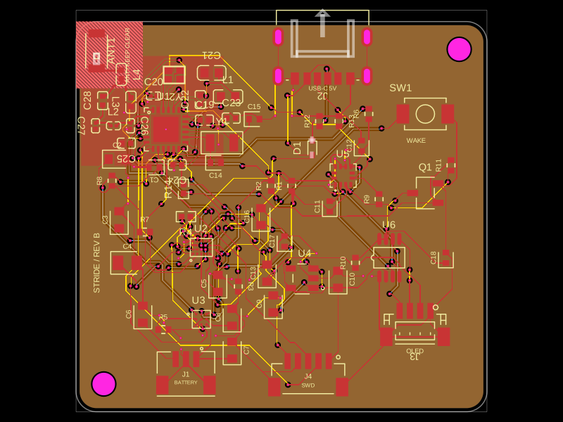 More from this authorimrishabh18/pedometerThis code defines and assembles a simple radio receiver hardware circuit using specific imported capacitors, inductors, RF connectors, and oscillator components with precise footprints and schematic attributes.
 Similar packagemohan-bee/esp32-c3This hardware design integrates an ESP32-C3 microcontroller, a USB-C connector, a power management IC (AP2112-3.3V regulator), a USB-to-Serial converter (CH340C), several resistors, capacitors, and user-accessible headers to facilitate USB communication, power regulation, and general I/O interfacing.
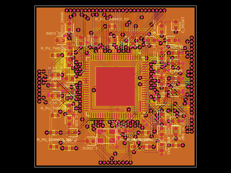 Discover something newastra/f1c100sThe code defines the physical pin layout, labels, and footprint for the F1C100S system-on-chip (SoC) component used in electronic devices.