imrishabh18/rp2040-motor-controller
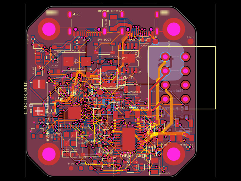
An RP2040-based NEMA17 stepper-motor controller with USB-C programming and PD motor-power negotiation, DRV8825 dual H-bridge drive, current/temperature telemetry, protected power filtering, status RGB LED, buzzer alarm, and optional magnetic encoder.
- Version
- 1.0.42
- License
- unset
- Stars
- 3
engineering/next-revision.md
> Historical revision record. Local v1.0.31 removes U_THERM_GATE and its support parts; see [current gate-removal notes](thermal-gate-removal.md).

# Next production revision — engineering checkpoint

Baseline: published imrishabh18/rp2040-motor-controller v1.0.21,
release d147f457-53fb-444e-9fa7-85ee390784e8, retrieved 2026-09-24.
The baseline is preserved in git commit e52b9b2. Changes are in index.circuit.tsx. This is NOT a production release.

## Confirmed requirements

- Revise the existing four-layer NEMA17 rear-cap PCB for the next manufactured batch.
- Provide actual current telemetry to the RP2040.
- Provide live current telemetry without claiming reliable blocked-motion detection.
- Add PD-voltage test access.
- Replace the single user indicator with a multicolor health/status indicator.
- Retain the outline and the existing motor, thermal shutdown, buzzer, USB and JST functions.
- Keep factory-populated components on top. Restore the optional bottom encoder footprint with doNotPlace.

## Encoder decision (updated after v1.0.22)

U_ENCODER (AS5600-ASOM) is restored at (0, 0) on the bottom and marked
`doNotPlace`. The factory assembly BOM and CPL exclude the sensor. Its two
bypass capacitors and two I²C pull-ups are on top and remain populated. GPIO0/1
are reserved for SDA/SCL. Fitting and using it later requires a shaft magnet,
alignment and application support. Current sensing remains independent.

## Current readout

Keep both existing 0.15-ohm DRV8847 sense resistors and current-limit configuration.
Add a separate 0.1-ohm, 1-W FRM121WFR100TM (JLC C7467250) in series with one lead
of each winding. This avoids interpreting a low-side regulation shunt as a continuous
phase-current measurement; winding recirculation may bypass the existing shunt.

For each new shunt, use an INA241A1IDDFR (JLC C19712054), gain 10 V/V, powered
from 3.3 V. Connect IN+ toward the driver and IN- toward the motor connector with
Kelvin sense routing. REF1 = 3.3 V, REF2 = GND sets the nominal zero-current output
to 1.65 V. Connect reserved pin 4 to GND per TI Table 5-1; the imported NC attribute
was corrected. Nominal transfer is Vout = 1.65 V + I_phase * 1 V/A. At +/-1 A,
nominal output is 0.65–2.65 V; shunt dissipation is 0.1 W at 1 A RMS.

Use GPIO28_ADC2 and GPIO29_ADC3. GPIO26/27 already serve the TMP102 I2C bus.
Local 100-nF supply bypass and a 1 kΩ / 10 nF output filter are fitted per channel (15.9 kHz nominal corner). Verify sampling bandwidth against actual commutation/PWM rates. Apply zero and gain
calibration and reject rail-clipped/invalid readings. This telemetry is not by itself
a stall detector. Input transient margins, temperature drift, resistor derating,
ADC settling, switching noise, and powered/unpowered states require bench checks.

## PD test access

index.circuit.tsx adds three top-side 1.5-mm probe pads with silkscreen:
- TP_PD: negotiated motor USB-C VBUS, before the fuse.
- TP_VMOTOR: protected motor supply, after F_MOTOR_VBUS.
- TP_PD_GND: common ground reference.

The raw PD pad must be labeled as PD, not as a guaranteed 5-V source. It follows
negotiation. Probe access and spacing must be reviewed on the final assembled board.
The current revision has its own regenerated, validated saved routing.

## RGB status indicator

LTST-C19HE1WT common-anode RGB LED (JLC C458749), exact imported footprint/CAD.
Use the programming USB's 5-V VBUS for LED supply, NOT the negotiated motor PD rail.
Switch each color with a DTC114EU3HZGT106 (JLC C509876) driven by an RP2040 GPIO;
this provides blue/green voltage headroom and avoids applying 5 V to a GPIO.
Use separate 1 kΩ current-limiting resistors per color. GPIOs: 25, 2, 3.
Check final supply tolerance, resistor values and brightness across LED bins.
The application defines color meanings and audible indications. Preserve the power indicator.

## Layout and verification status

- Typecheck passes after fixing original symbol props/duplicate style and recording a local fanout-solver type compatibility patch.
- Electrical tests pass: physical amplifier pin mapping, separate winding/ADC nets, retained 0.15 Ω limit shunts, RGB isolation from PD, probe connectivity, DNP bottom encoder wiring, common GND.
- Final standard CLI build passes. Embedded DRC and an independent routing-check pass both report zero errors.
- `tsci check`: 0 errors, 166 warnings (catalog/metadata, trace-length and schematic styling guidance). These warnings are retained and visible; this is not a warning-free build.
- Gerber-based shorts check: no shorts across all four copper layers.
- Physical ground audit: 1 connected network, containing all ground pads, mounting rings, traces, vias and 12 retained pour regions. No separate ground island remains.
- 19 Bun tests pass, covering net connectivity, mechanical constraints, routing, thermal interlocks, eight schematic sheets and stale-geometry guards. Typecheck passes.
- Netlist and PCB placement checks report zero errors; PCB placement retains eight orientation suggestions. Schematic analysis still offers layout heuristics, including generic-box warnings on the USB custom symbol; the new current and RGB sheets were visually reviewed.
- Board remains 42.30 × 42.32 mm, four copper layers, with all populated components on top. Only the optional DNP encoder footprint is on the underside; its support parts are on top.
- Bench calibration, PWM/transient/noise checks, current bandwidth and LED brightness verification remain necessary on the prototype.
- Registry publication shares this engineering iteration; it is not a production qualification. No order or production-ready fabrication export was performed.

## Primary references

- https://www.ti.com/lit/ds/symlink/drv8847.pdf
- https://www.ti.com/lit/ds/symlink/ina241a.pdf
- https://www.ti.com/lit/an/slvaei3a/slvaei3a.pdf
- https://optoelectronics.liteon.com/upload/download/DS22-2008-0044/LTST-C19HE1WT_20210326.PDF
- https://www.rohm.com/products/transistors/digital-transistors/automotive/dtc114eu3hzg-product

## Compact current-limit resistors

R_ISEN_A/B retain 0.15 Ω and 1% tolerance, but use HoLRT1206-1W-150mR-1%
(JLC C5127776) instead of the earlier 2512 3 W parts. At the nominal 1 A limit,
I²R is 0.15 W; even a 1.15 A threshold is about 0.20 W. The selected 1 W rating
is specified at 70°C; the manufacturer's curve requires derating above 70°C.
Check resistor temperature on the prototype; a board-sensor threshold is not a
measurement of the resistor's internal temperature. Do not raise motor current
without recalculating resistor dissipation and driver/trace thermal limits.

Manufacturer series datasheet (hosted by DigiKey):
https://mm.digikey.com/Volume0/opasdata/d220001/medias/docus/6474/HoLRT1225-3W-1R-5%25.pdf

The imported NPN, amplifier and LED courtyards were normalized to centred body/pad
envelopes with at least 0.25 mm margin. Copper pads and CAD alignment are unchanged.
DTC114EU3HZG uses a 3.3 × 2.9 mm courtyard, INA241 DDF 4.25 × 3.6 mm,
and LTST-C19HE1WT 2.45 × 3.1 mm. This removes asymmetric library whitespace,
not the physical placement clearance.

## Routing and ground-pour finalization

The Pipeline 7 routes were repaired locally using clearance-aware searches and
expanded for motor current. All six winding-current paths are checked, including
the new shunt-to-connector segments. Minimum neck width is 0.350 mm, confined to
package escapes; any continuous segment below 0.5 mm is under 1.5 mm long.
At 20°C and a conservative assumed 18 µm copper thickness on every layer,
individual trace resistance estimates are 0.010–0.036 Ω, excluding vias, pads and
shunts. These calculations are regression checks, not proof of thermal capacity;
verify the actual fabrication stack and test at the intended motor current.
All vias span the board, with 0.3 mm drill and 0.45 mm pad; no blind/buried vias.

The net-wide requested-width checker reports 101 advisories on 34 physical traces,
including repeated reports for shared supply escapes. The hard 0.1 mm clearance
rule is unchanged. Motor-path width, narrow-run length and estimated resistance
have independent regression checks instead of relying on the advisory count.

The pinned core pour generator produced 100 floating copper fragments despite
connecting all ground terminals. `routing/ground-pour-selection.json` records the
independent physical audit's selection. The board removes those actual fragments
before normal DRC, preview and export. It does not remove errors or suppress checks.
A geometry change rejects the selection and requires a new audit, just as saved
routing rejects changed terminal geometry. Twelve connected regions remain, joined
through copper traces and plated vias into one physical ground network.

For a changed layout, render a new candidate with `scripts/reroute-revision.tsx`
(or `scripts/render-route-plan.tsx` after local route edits). Candidate renders
skip the fixed pour selection. Run `scripts/audit-ground-copper.py` with Shapely
against that candidate, inspect any disconnected groups, then run
`scripts/save-ground-pour-selection.py`. The latter refuses to remove groups
containing a pad, trace or via. Copy the validated candidate plan to
`routing/route-plan.json`, build normally, and repeat the full checks and physical
ground audit. An audit of raw floating pours intentionally exits unsuccessfully.

Before a production release, calibrate current zero/gain with real hardware,
check both polarities and PWM/recirculation, thermals and power sequencing, and
review the supplier's assembly preview for the newly added packages. Existing
SOT-23 placement corrections in the assembly exporter remain part-specific;
CAD model rotation is not evidence of the supplier's placement rotation.

## 12 V motor supply configuration — 2026-09-25

R_PD_CFG1 changes from 6.8 kΩ to 24 kΩ, 1%, 0603 (UNI-ROYAL
0603WAF2402T5E, JLC C23352). CH224K resistor mode requests 12 V with this value;
CFG2 and CFG3 remain unconnected. Use a PD source advertising 12 V. This is a
hardware request, not a firmware voltage setting or a guarantee of the source's
available profiles. The winding current limit is unchanged.

D_MOTOR_TVS changes from SMBJ11CA to Diodes SMBJ13CA-13-F (JLC C135043),
retaining the SMB footprint. Its 13 V reverse stand-off accommodates a 12 V rail
up to +5% (12.6 V); the old 11 V stand-off part was unsuitable for that range.
DRV8847's recommended VM range extends to 18 V (20 V absolute maximum).
The existing 25 V ceramic capacitors and 30 V fuse accommodate 12 V. The
16 V polymer bulk capacitor is retained for nominal operation; verify its
voltage/temperature derating and regenerative voltage rise on the prototype.

The replacement TVS specifies up to 21.5 V at its rated surge current. Therefore
it does NOT guarantee protection below either the driver's 20 V absolute maximum
or the bulk capacitor's 16 V rating. Do not treat the DRC pass as transient
qualification: scope hot-plug and worst-case motor regeneration before production;
if the rail exceeds component limits, a coordinated clamp/braking circuit and/or
higher-rated parts are required. This voltage configuration is not surge-certified.

References:
- [WCH CH224 datasheet, resistor-mode table](https://aitendo3.sakura.ne.jp/aitendo_data/product_img/ic/power/CH224K/CH224K.PDF)
- [24 kΩ assembly resistor](https://jlcpcb.com/partdetail/0603WAF2402T5E/C23352)
- [Diodes SMBJ13CA specifications](https://www.diodes.com/part/view/SMBJ13CA)
- [Replacement TVS assembly part](https://jlcpcb.com/partdetail/DiodesIncorporated-SMBJ13CA_13F/C135043)
- [TI DRV8847 datasheet](https://www.ti.com/lit/ds/symlink/drv8847.pdf)

## Superseded supply setting — 2026-09-26

The 12 V setting above is historical. The active design now retains DRV8847 and
requests 15 V; see [15v-pd.md](15v-pd.md) for changed parts and outstanding
transient qualification. The 20 V/TMC2209 exploration was abandoned.

## 20 V DRV8825 successor

The 12/15 V configurations above are historical. The active source has migrated
to DRV8825 and 20 V PD; see [20v-drv8825.md](20v-drv8825.md). Earlier validation
results do not qualify this changed hardware.
Related Packages
 More from this authorimrishabh18/3d-model-testIt loads a 3D model of an electronic component onto a circuit board with specified positioning.
 Similar packageastra/nema17-stepper-motor-controller-spring-clamp-rp2040A 4-layer RP2040 controller board that negotiates USB‑C PD motor power and drives a NEMA17 stepper via a DRV8825, with current sensing, thermal shutdown, RGB status LED, buzzer alarm, optional AS5600 encoder, protection/filtering, and test points.
 Discover something newseveibar/am3352-dev-board-4layer-dogboneDefines PCB footprints and pin mappings for a TI AM3352ZCZ100 processor, JST GH connectors, and assembly-part lookup helpers for capacitors, resistors, and headers.