imrishabh18/rp2040-motor-controller
An RP2040-based NEMA17 stepper-motor controller with USB-C programming and PD motor-power negotiation, DRV8825 dual H-bridge drive, current/temperature telemetry, protected power filtering, status RGB LED, buzzer alarm, and optional magnetic encoder.
- Version
- 1.0.42
- License
- unset
- Stars
- 3
engineering/jlc-ic-footprint-audit.md
> Historical revision record. Local v1.0.31 removes U_THERM_GATE and its support parts; see [current gate-removal notes](thermal-gate-removal.md).

# JLCsearch IC-footprint audit and DRC clarification

The revised local board uses supplier imports for important ICs. Standard passive footprint strings remain unchanged, as requested. This update has not been pushed; the online version remains v1.0.27.

## Changes and verification

- **RP2040 MCU, W25Q16 flash, AP2112 regulator:** explicit references to freshly imported, exact EasyEDA pad geometry. Existing names, pin aliases and electrical connections are preserved.
- **DRV8825:** explicit reference to the fresh JLCsearch import. This retains the importer-generated matched land pattern (99.1% mean per-pin copper overlap with the raw supplier pads). The raw library additionally contains 12 unconnected via-in-pad holes; these were not introduced into this board. The existing board-level thermal vias remain.
- **Q_PD_ENABLE / BSS84 / C85202:** replaced the generic SOT-23 footprint with the exact supplier import. Rotation changed from 90° to 270° to preserve the physical pin orientation; the old 180° assembly correction was removed, so final placement rotation remains 270°.
- The other active-device land patterns—including TMP102, CH224K, INA241, logic gate, buzzer transistor, status transistors and optional AS5600—match the supplier pads exactly after accounting for orientation and bottom-side mirroring.
- Pin numbers agree for every audited part. Passive pads, board outline, vias, source nets and source connectivity are unchanged. Trace endpoints were aligned to the imported pad centers, and connected ground-pour selection was regenerated and audited.

## Validation

TypeScript, source netlist, schematic placement, PCB placement, build validation and all 20 circuit tests pass. The final built board has zero embedded DRC errors. Gerber-derived shorts checks and an independent all-net copper audit found no shorts or unintended open nets. Existing warnings and fabrication findings are not suppressed.

## Why the UI shows no clearance errors

| Check | Board configuration / result | Separate manufacturer check |
|---|---|---|
| Via-hole edge-to-edge spacing | 0.10 mm minimum; smallest measured gap is 0.10 mm | JLCPCB lists 0.20 mm; six pairs are below this |
| Via-hole-to-track / inner copper | Passing the current routing rules does not establish this separate drilling clearance | JLCPCB lists 0.20 mm; 171 per-layer/object comparisons remain below it, across 112 vias |

These are **separate fabrication-rule findings, not errors displayed by the existing tscircuit DRC configuration**. The earlier wording should not have implied otherwise. JLCPCB lists copper-to-copper and drill-to-copper rules separately; they are not interchangeable. [JLCPCB capabilities](https://jlcpcb.com/capabilities/Capab)

Using a standard passive footprint string is permitted by the requested scope; a generic-passive footprint mismatch warning is not by itself evidence of an incorrect package. The separate drill-spacing findings remain unresolved by this IC-footprint update.
Related Packages
 More from this authorimrishabh18/3d-model-testIt loads a 3D model of an electronic component onto a circuit board with specified positioning.
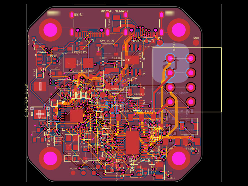 Similar packageastra/nema17-stepper-motor-controller-spring-clamp-rp2040A 4-layer RP2040 controller board that negotiates USB‑C PD motor power and drives a NEMA17 stepper via a DRV8825, with current sensing, thermal shutdown, RGB status LED, buzzer alarm, optional AS5600 encoder, protection/filtering, and test points.
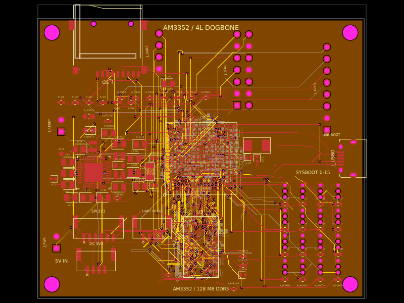 Discover something newseveibar/am3352-dev-board-4layer-dogboneDefines PCB footprints and pin mappings for a TI AM3352ZCZ100 processor, JST GH connectors, and assembly-part lookup helpers for capacitors, resistors, and headers.