imrishabh18/rp2040-motor-controller
An RP2040-based NEMA17 stepper-motor controller with USB-C programming and PD motor-power negotiation, DRV8825 dual H-bridge drive, current/temperature telemetry, protected power filtering, status RGB LED, buzzer alarm, and optional magnetic encoder.
- Version
- 1.0.42
- License
- unset
- Stars
- 3
engineering/jlc-clearance-update-v1.0.37.md
# JLCPCB clearance update — v1.0.37

Target: four layers, **1 oz outer copper / 0.5 oz inner copper**, with the existing 1.6 mm board thickness. These checks do not cover the larger spacing required by a 2 oz order.

## Clearance changes

- Remove all 37 power-to-pad spacing exceptions from v1.0.36. Every audited motor-power route must meet 0.15 mm to foreign pads; the previous general 0.10 mm minimum remains appropriate for ordinary 1 oz signal routing.
- Reposition tight route corners and locally resize broad copper. Preserve the winding-path limits on width, narrow-escape length, total length, via count and estimated resistance. The nominal winding-current setting stays approximately 1 A peak.
- Move the two vias that were below the board's 0.125 mm via-to-pad target and check foreign trace clearance from the drilled hole on every layer.
- Correct both USB-C locating drills from the builtin 0.70 mm to the manufacturer-drawn 0.65 mm, retaining their centres. Round contact-land corners by 0.075 mm without shortening the lands; move nearby tracks and provide 0.21 mm nominal pour clearance to prevent polygon approximation from falling below 0.20 mm.
- Keep every test point and component. No functional connection, component value or current-limit setting changes.

## Rules and verification

The machine-readable profile is [jlcpcb-clearance-rules.json](jlcpcb-clearance-rules.json), based on [JLCPCB's rigid PCB capabilities](https://jlcpcb.com/capabilities/pcb-capabilities). The [standard copper guide](https://jlcpcb.com/blog/copper-weight-and-trace-width-balance) describes 1 oz outer and 0.5 oz inner copper for multilayer boards.

| Check | Minimum |
|---|---:|
| Signal track width, track-to-track and pad-to-track | 0.10 mm |
| Component pad-to-pad; motor-power track-to-pad | 0.15 mm |
| Via-to-pad board target | 0.125 mm |
| Via drill-to-foreign-track; inner via drill-to-copper | 0.20 mm |
| Plated component drill-to-foreign-track | 0.28 mm |
| Inner plated component drill-to-foreign-copper | 0.30 mm |
| NPTH-to-copper; routed board edge-to-copper | 0.20 mm |
| Via drill-to-via drill | 0.20 mm |
| Plated component drill-to-other plated drill | 0.45 mm |

The native checker currently uses the component pad-spacing field for via-to-pad spacing too. The board sets that shared field to 0.125 mm and the independent `checkJlcClearances` gate separately enforces 0.15 mm between component pads. No reported DRC errors are deleted or suppressed. The old 37-entry exception list is empty and the integration test requires zero exceptions.

The manufacturing audit independently checks physical copper connectivity, shorts and drill clearances. Its via-hole check now accumulates results from all four layers rather than retaining only the last layer's results. The delivered Gerbers and NPTH Excellon file are also checked independently, including the rounded-pad aperture macros and dark/clear pour polarity. Floating pour fragments are excluded only after proving that they contain no component pad, trace or via.

See [revision-checks.json](revision-checks.json) for the final artifact hashes, actual results and warning counts. Run the TypeScript checks plus `audit-manufacturing.py`, `audit-ground-copper.py` (all layers and outer layers), `audit-kelvin-connections.py`, `audit-driver-thermal-vias.py` and `audit-exported-clearances.py` after rebuilding and exporting.

## Fabrication hold: USB-C connector qualification

**Clearance approval is not approval to order this assembly at 20 V.** Both USB-C connectors remain SHOUHAN TYPE-C 16PIN 2MD(073), C2765186. Its [manufacturer drawing](https://datasheet.lcsc.com/datasheet/pdf/2d53d8d8199c9dd6666d9bc9ac7c3a1e.pdf?productCode=C2765186), page 1, explicitly rates it **5 V, 3 A**. A 100 V dielectric withstand test does not establish a 20 V operating rating. Replace the PWR connector with a suitably rated part, or obtain written manufacturer qualification, before ordering for 9–20 V PD use.

The same drawing labels its recommended PCB layout as 0.8 mm thick. The board remains 1.6 mm, so retention-leg fit and the assembly process also require confirmation. The copper-clearance edits do not resolve that mechanical question.

[JLCPCB C165948 / HRO TYPE-C-31-M-12](https://jlcpcb.com/partdetail/Korean_HropartsElec-TYPE_C_31_M12/C165948) is a candidate rated 20 V / 5 A, but it has **not** been substituted or mechanically validated in this revision. Compare its exact supplier footprint and manufacturer drawing before use.

Other existing first-board conditions remain: no firmware is bundled; application software owns temperature thresholds and PD transitions; the approximately 1 A peak current setting is unchanged; validate bus overshoot, regeneration, thermal rise and current telemetry on hardware. Historical v1.0.36 fabrication-readiness wording is superseded by this connector hold.
Related Packages
 More from this authorimrishabh18/3d-model-testIt loads a 3D model of an electronic component onto a circuit board with specified positioning.
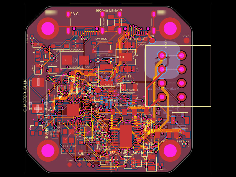 Similar packageastra/nema17-stepper-motor-controller-spring-clamp-rp2040A 4-layer RP2040 controller board that negotiates USB‑C PD motor power and drives a NEMA17 stepper via a DRV8825, with current sensing, thermal shutdown, RGB status LED, buzzer alarm, optional AS5600 encoder, protection/filtering, and test points.
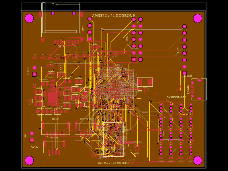 Discover something newseveibar/am3352-dev-board-4layer-dogboneDefines PCB footprints and pin mappings for a TI AM3352ZCZ100 processor, JST GH connectors, and assembly-part lookup helpers for capacitors, resistors, and headers.