imrishabh18/rp2040-motor-controller
An RP2040-based NEMA17 stepper-motor controller with USB-C programming and PD motor-power negotiation, DRV8825 dual H-bridge drive, current/temperature telemetry, protected power filtering, status RGB LED, buzzer alarm, and optional magnetic encoder.
- Version
- 1.0.41
- License
- unset
- Stars
- 3
engineering/configurable-pd.md
# RP2040-controlled CH224K voltage selection — v1.0.33

CH224K is retained. Its three configuration pins now connect to three inverting,
open-collector DTC114EETL buffers (ROHM, JLCPCB C79605), each with a 47 kΩ
0402 pull-up (C25792) to **CH224K VDD**, not MCU 3.3 V. The transistors use the
exact JLCsearch/EasyEDA copper footprint; their schematic symbols show the
internal 10 kΩ input and base/emitter resistors.

The DATA USB powers RP2040. The PWR USB independently powers CH224K. The
buffer collector/base isolation avoids a forward-biased GPIO clamp path between
these domains when either cable is absent. Common GND is retained. An unpowered
or high-impedance MCU leaves the transistor inputs low through their internal
resistor networks; the CFG pull-ups request 5 V. GPIO-high turns its transistor
on and pulls the corresponding CFG input low. This is an **inverting interface**.

| Signal | RP2040 GPIO / physical pin | Buffer | CH224K physical pin |
|---|---|---|---|
| PD_CFG1_LOW | GPIO4 / pin 6 | Q_PD_CFG1 | CFG1 / pin 9 |
| PD_CFG2_LOW | GPIO5 / pin 7 | Q_PD_CFG2 | CFG2 / pin 2 |
| PD_CFG3_LOW | GPIO6 / pin 8 | Q_PD_CFG3 | CFG3 / pin 3 |

CH224K's exposed GND pad is represented by pin 11 in the supplier import.
DTC114EETL is pin 1=input, pin 2=GND/emitter, pin 3=output/collector.
The earlier screenshot's assignment CFG1=2, CFG2=3, CFG3=9 is incorrect for CH224K.

| Requested supply | GPIO4 | GPIO5 | GPIO6 | Actual CFG1/2/3 |
|---|---:|---:|---:|---|
| 5 V (reset/default) | 0 | 0 | 0 | 1 / 1 / 1 |
| 9 V | 1 | 1 | 1 | 0 / 0 / 0 |
| 12 V | 1 | 1 | 0 | 0 / 0 / 1 |
| 15 V | 1 | 0 | 0 | 0 / 1 / 1 |
| 20 V | 1 | 0 | 1 | 0 / 1 / 0 |

These are PD requests, not guaranteed adapter outputs. The adapter must support
the requested profile and enough current. This circuit does not add PPS, I2C
control, or readback of the adapter's advertised profiles.

## Application contract

No device firmware is included in this PCB package. Application software must
configure the new GPIOs before requesting motor operation. Older firmware that
leaves them as inputs keeps the PWR supply at 5 V, which cannot operate DRV8825.

1. Hold GPIO22 low and stop STEP pulses before selecting or changing voltage.
2. Start the three selector GPIOs low. To change a preset, first set GPIO4 low
   (5 V request), update GPIO5/6, then set GPIO4 high for the chosen non-5 V
   profile. Do not leave sequential intermediate voltage codes while running.
3. Keep the motor asleep through renegotiation and settling. Characterize the
   required delay with the intended adapter; GPIO22 must not be raised during
   the transition. The existing CH224K PG / BSS84 interlock remains in series
   with nSLEEP, but PG is **not connected to an MCU input**. Firmware cannot use
   this board to read PG or automatically verify actual VBUS.
4. Validate TP_PD and TP_VMOTOR before enabling operation. DRV8825 needs at least
   8.2 V at VM. Prefer 12/15/20 V; at 9 V, cable/fuse/diode losses may leave
   insufficient margin. Do not run the motor at the 5 V startup setting.
5. When reducing voltage, the reverse-blocking diode can leave the motor
   capacitors charged above the new PD voltage. Keep the motor asleep until
   TP_VMOTOR has settled; a PD request alone does not discharge the rail.

The existing ~1 A peak current limit, INA240 sensing, temperature telemetry,
thermal vias, PG interlock, and 20 V-rated power architecture are retained.
No external thermal shutdown gate is added.

## Design calculations and bench verification

At 3.36 V and −1% pull-up tolerance, each 47 kΩ pull-up supplies at most 72.2 µA;
all three sinking adds about 217 µA to CH224K VDD load. The existing 1 kΩ VDD
feed resistor remains. The ROHM transistor's specified off leakage is 500 nA at
50 V and 25 °C (24 mV across 47 kΩ); its guaranteed switching specifications
comfortably exceed this small collector load at a 3.3 V MCU input. WCH does not
specify every CFG leakage/startup timing parameter. Scope CFG1/2/3 and VDD at
cold start and through transitions; confirm the intended 5 V startup under both
cable insertion orders and MCU reset/brownout. Check both power rails with one
USB cable removed. These electrical/PCB checks do not replace a prototype test.

All six added parts are on top. Two existing debug test pads (TP_SWCLK and
TP_GND) move 1 mm toward the bottom edge to make room. R_PD_VBUS moves above the MCU and uses a 10 kΩ 0402 C25744 footprint to clear the GPIO escape paths. Its worst-case dissipation with the entire 21 V across 9.9 kΩ is 44.6 mW, below its 62.5 mW rating; the normal sensed-pin voltage reduces this load. The optional bottom
encoder remains unpopulated.

## Sources

- [WCH CH224 datasheet V2.0, pinout and CH224K table in §6.2](https://done.land/assets/files/ch224aq_datasheet.pdf)
- [WCH original CH224K datasheet, dynamic GPIO configuration and startup caveat in §5.2.2](https://components101.com/sites/default/files/component_datasheet/WCH_CH224K_ENG.pdf)
- [ROHM DTC114EETL datasheet](https://fscdn.rohm.com/en/products/databook/datasheet/discrete/transistor/digital/dtc114eetl-e.pdf)
- [JLCsearch C79605](https://jlcsearch.tscircuit.com/components/list?search=C79605)
- [TI DRV8825 datasheet](https://www.ti.com/lit/ds/symlink/drv8825.pdf)
Related Packages
 More from this authorimrishabh18/3d-model-testIt loads a 3D model of an electronic component onto a circuit board with specified positioning.
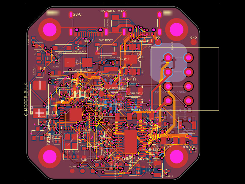 Similar packageastra/nema17-stepper-motor-controller-spring-clamp-rp2040A 4-layer RP2040 controller board that negotiates USB‑C PD motor power and drives a NEMA17 stepper via a DRV8825, with current sensing, thermal shutdown, RGB status LED, buzzer alarm, optional AS5600 encoder, protection/filtering, and test points.
 Discover something newseveibar/am3352-dev-board-4layer-dogboneDefines PCB footprints and pin mappings for a TI AM3352ZCZ100 processor, JST GH connectors, and assembly-part lookup helpers for capacitors, resistors, and headers.