imrishabh18/rp2040-motor-controller
An RP2040-based NEMA17 stepper-motor controller with USB-C programming and PD motor-power negotiation, DRV8825 dual H-bridge drive, current/temperature telemetry, protected power filtering, status RGB LED, buzzer alarm, and optional magnetic encoder.
- Version
- 1.0.41
- License
- unset
- Stars
- 3
engineering/20v-drv8825.md
> Historical power-stage design notes. v1.0.33 retains this driver/power stage but replaces the fixed 20 V straps with GPIO-selectable PD, relocates R_PD_VBUS and uses a 0402 C25744 for that 10 kΩ sense resistor. See [current PD interface](configurable-pd.md) and [current validation](revision-checks.json).

# 20 V PD / DRV8825 revision — 2026-09-26

This revision replaces DRV8847 with TI DRV8825PWPR (C81582). It implements the
requested 20 V PD supply while preserving the 42.30 × 42.32 mm, four-layer motor
cap, top-side assembly, current telemetry, temperature telemetry, buzzer, RGB
indicator and optional bottom AS5600 (do-not-place, excluded from BOM/CPL).
The 12 V and 15 V notes are historical. No TMC2209 is used.

## Power and current

- CH224K CFG1, CFG2 and CFG3 are deliberately open. **For CH224K**, resistor-mode
  CFG1 open requests 20 V. This differs from newer CH224A/Q variants: do not
  substitute those parts without redesigning the configuration.
- A PD source advertising a 20 V fixed PDO is required. The motor rail is the
  negotiated voltage less the reverse-blocking diode's load-dependent drop.
- R_PD_VDD is 1 kΩ, 750 mW, CRCW12061K00FKEAHP (C844867, 1206). At 21 V input,
  3.0 V VDD and 990 Ω, dissipation is 327 mW. Check its temperature on hardware.
- The 2 A / 30 V PTC remains on the input side. PMEG6020ELRX (C478000, 60 V,
  2 A) follows it, anode towards the fuse and cathode towards VMOTOR. This blocks
  reverse motor-rail current into the PD port; it is not an active braking circuit.
- D_MOTOR_TVS is SMBJ22CAQ-13-F (C1975329): 22 V stand-off and 35.5 V rated
  pulse clamp. All motor-rail capacitors are now 50 V. The clamp is below the
  DRV8825's 45 V operating / 47 V absolute limits under its specified pulse
  conditions. Layout inductance and sustained regeneration still require testing.
- C_MOTOR_BULK is TCJD226M050R0090E (C5981428), **22 µF / 50 V**, 7.3 × 4.3 mm
  D case, 2.9 mm nominal / 3.1 mm maximum high. C_PD_VBUS and C_VM_BULK are
  10 µF / 50 V CL31A106KBHNNNE (C13585); their effective capacitance falls under
  DC bias. This is substantially less bulk energy storage than the earlier
  100 µF / 25 V or 220 µF / 16 V parts. Ripple, hot-plug and regeneration tests
  are required; increase capacitance or add active braking if measurements demand it.
- The C5981428 supplier catalog entry has no importable EasyEDA component.
  Its geometry and CAD model reuse the identical manufacturer TCJ D case imported
  for C2159920. The BOM and electrical ratings identify the actual 50 V part.
  Inventory was checked, but is not reserved.

DRV8825 current regulation uses independent **0.3 Ω, 1 W** shunts (C5127777).
The 2.4 kΩ / 2 kΩ divider from V3P3OUT produces nominally 1.5 V:

`I_FS = VREF / (5 × R_ISENSE) = 1.5 / (5 × 0.3) = 1.0 A peak`

The driver reference supply remains separate from the MCU's 3.3 V rail. Its
worst-case divider + MODE2 + reference-input load is below 1 mA. The 1 A value
is nominal: account for regulator, resistor and current-regulation tolerances
when qualifying the actual motor. Higher supply voltage does not authorize a
higher winding-current setting. The cost-reduced revision uses separate inline 0.05 Ω shunts and INA240A1
amplifiers (20 V/V); the nominal ADC scaling remains 1 V/A.

## Driver support and control interface

- Both VMA/VMB connect to VMOTOR and have 100 nF / 50 V local bypasses.
- CP1–CP2: 10 nF / 50 V; VCP–VM: 100 nF / 50 V with 1 MΩ in parallel.
- V3P3OUT: 470 nF / 16 V. VREF: 100 nF filtering.
- MODE2 high, MODE1/MODE0 low selects fixed **1/16 microstepping**. DECAY open
  selects mixed decay. NC and nHOME stay unconnected. nHOME is an indexer state,
  not a shaft encoder or limit switch.
- Ten 0.30/0.50 mm thermal vias now sit inside the exposed pad, joining solid
  inner and bottom GND copper. Six perimeter vias remain. Preserve bottom tenting;
  see [thermal-via fabrication notes](drv8825-thermal-vias.md).
- TMP102 remains next to the larger package; sensor-to-driver center distance
  is 5.7 mm. The old 5 mm center-distance rule assumed the smaller driver package.

| Signal | RP2040 GPIO | DRV8825 physical pin |
|---|---:|---:|
| STEP | 18 | 22 |
| DIR | 19 | 20 |
| nRESET | 20 | 16 |
| nENBL | 21 | 21 |
| MCU enable, through PD + temperature telemetrys | 22 | nSLEEP, 17 |
| nFAULT | 23 | 18 |

The DRV8825 uses STEP/DIR control. The application must handle nRESET, nENBL,
the USB-PD gated enable input and nFAULT according to the driver datasheet.
For a 1.8° motor, the fixed 1/16 mode has 3200 commanded microsteps per revolution.
Sleep removes holding torque and resets the driver indexer; application control
must account for this. Current measurement does not establish shaft movement.
GPIO25 is assigned to the red LED channel. Device firmware is supplied separately.

## Qualification status

The current INA240 revision is 1.0.31. It removes the external thermal gate while retaining the ten in-pad thermal vias. It passes typechecking, 21 circuit tests (2290 assertions), native routing DRC, all-layer Gerber short checks, and independent physical connectivity/drill checks. `tsci check` reports 0 errors and 169 warnings. Eight retained ground pours form one physical network; 99 floating pour-only fragments were removed. See [INA240 revision](ina240-revision.md) and [revision-checks.json](revision-checks.json) for the checked artifact, warning scope and hashes.

The assembly export has 101 top-side parts, no bottom-side assembly, and excludes the DNP encoder and bare holes/test pads. Supplier pin-1 metadata remains incomplete, so check assembly orientation in the ordering preview. Existing verified SOT-23 offsets remain. CAD-model rotation is not an assembly rotation instruction. This local revision has not been published or tested on physical hardware.

Before production: verify 20 V negotiation/fallback, VM ramp (<1 V/µs), hot-plug
and back-drive peaks, diode/PTC temperature, both winding limits, current-sensor
calibration, microstep waveform quality at low speed (DRV8825 blanking time),
application temperature and fault handling and loss of PD. Test with the actual
motor, cable, charger and enclosure. A transient-rated TVS cannot absorb
continuous back-driving power indefinitely.

## References

- [TI DRV8825 datasheet](https://www.ti.com/lit/ds/symlink/drv8825.pdf), pins,
  current regulation, timing, support circuit and layout.
- [WCH CH224 manufacturer datasheet, mirrored PDF](https://w2.electrodragon.com/Chip-cn-dat/WCH-dat/CH224-dat/ch224ds1.pdf), §5.2.1 and §6.1.
- [Nexperia PMEG6020ELR datasheet](https://assets.nexperia.com/documents/data-sheet/PMEG6020ELR.pdf).
- [KYOCERA AVX TCJ series](https://datasheets.kyocera-avx.com/TCJ.pdf), D-case
  dimensions and TCJD226M050#0090E rating.
- [Vishay CRCW-HP information](https://www.vishay.com/docs/48621/_infographic-crcw-hpe3.pdf).

- [Diodes Incorporated SMBJ22CAQ ratings](https://www.diodes.com/part/view/SMBJ22CAQ).
Related Packages
 More from this authorimrishabh18/3d-model-testIt loads a 3D model of an electronic component onto a circuit board with specified positioning.
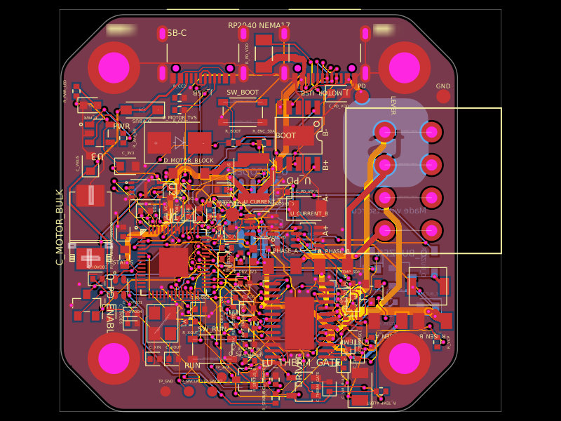 Similar packageastra/nema17-stepper-motor-controller-spring-clamp-rp2040A 4-layer RP2040 controller board that negotiates USB‑C PD motor power and drives a NEMA17 stepper via a DRV8825, with current sensing, thermal shutdown, RGB status LED, buzzer alarm, optional AS5600 encoder, protection/filtering, and test points.
 Discover something newseveibar/am3352-dev-board-4layer-dogboneDefines PCB footprints and pin mappings for a TI AM3352ZCZ100 processor, JST GH connectors, and assembly-part lookup helpers for capacitors, resistors, and headers.