imrishabh18/rp2040-motor-controller
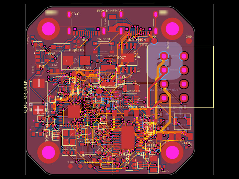
An RP2040-based NEMA17 stepper-motor controller with USB-C programming and PD motor-power negotiation, DRV8825 dual H-bridge drive, current/temperature telemetry, protected power filtering, status RGB LED, buzzer alarm, and optional magnetic encoder.
- Version
- 1.0.41
- License
- unset
- Stars
- 3
README.md
# RP2040 NEMA 17 motor cap with temperature and current telemetry

This package contains the PCB design, circuit checks and fabrication outputs. No device firmware is included.

The local fabrication update following **v1.0.39** refreshes the saved routing for the current core, shortens decoupling connections, and repairs copper clearances. Capacitor and nearby passive placements have changed. The optional encoder and its two bypass capacitors are unpopulated on the bottom. See [the routing review](reports/routing-refresh-review.md) and [current validation](reports/validation.json); `engineering/revision-checks.json` describes the earlier board. This update includes the validated routing and clearance repairs.

Revision **1.0.41** applies the copper-contact checker fix from [checks PR #371](https://github.com/tscircuit/checks/pull/371) as a temporary dependency patch. It lets the published build complete DRC when separate copies of the geometry library are loaded. The PCB copper and Gerber ZIP are unchanged from 1.0.40; this revision updates the generated diagnostics.

Revision **1.0.38** replaced both USB-C receptacles with **HRO TYPE-C-31-M-12 / C165948**, rated **20 V / 5 A**, using the exact JLCsearch/EasyEDA supplier footprint and 3D model. See [USB-C replacement and validation](engineering/usb-c-20v-v1.0.38.md).

The preceding v1.0.37 removed all 37 power-clearance exceptions and added explicit JLCPCB 1 oz fabrication rules. Its old C2765186 connector hold is superseded by the replacement in this revision. v1.0.36 imported all twelve DRV8825 thermal vias directly from C81582’s exact EasyEDA footprint, removing both manually added arrays.

The new connector rating covers the intended 20 V PD request. The board remains 1.6 mm thick; the HRO drawing describes a top-mounted connector and does not specify a 0.8 mm PCB restriction. Its shell stakes are approximately 1.01 mm long, so assembly must solder them within the plated slots on this board. Review those joints and placement in the JLCPCB assembly preview. No powered prototype testing has been performed.

Revision **1.0.35** moves motor USB-PD supply, winding and regulation-shunt tracks to the top/bottom layers. Kelvin sensing, solid copper around the driver thermal vias, and connected outer-layer ground returns are retained. See [outer-layer routing notes](engineering/outer-layer-power-routing.md).

Revision **1.0.34** removed R_TEMP_ALERT and disconnected TMP102 ALERT from GPIO24. The RP2040 reads temperature over I²C and generates alerts in application software. GPIO24 is unused. See [I²C-only temperature update](engineering/i2c-temperature-alerts.md).

Revision **1.0.33** adds RP2040 control of the CH224K voltage selection through GPIO4/5/6 and three inverting transistor buffers. Startup requests 5 V; application software can request 9/12/15/20 V. See [configurable PD wiring and application requirements](engineering/configurable-pd.md). The schematic explanations added in v1.0.32 are retained.

Revision **1.0.31** removes the external thermal AND gate and connects the existing MCU/USB-PD enable path directly to DRV8825 nSLEEP. At that revision TMP102 retained its ALERT input to the MCU; v1.0.34 now uses I²C readings only. Ten in-pad driver thermal vias and the INA240A1DR current-sensing circuit are retained. See [gate removal](engineering/thermal-gate-removal.md).

A 42.30 × 42.32 mm, four-layer, 1.6 mm PCB based on the [PD-Stepper V1.1 mechanical outline](https://github.com/joshr120/PD-Stepper). Four 3.3 mm mounting holes sit on a 31 × 31 mm square. The four mounting rings, MCU, driver and temperature circuit share one GND net.

The smaller board replaces the original screw terminal with a top-entry **JST PH 4-pin, 2 mm-pitch connector**, B4B-PH-K-S(LF)(SN). Pin order is A+, A−, B+, B−; use a matching PHR-4 motor cable. USB and component placement have been rearranged. Top and bottom have ground pours; the two inner layers carry routed connections and local ground patches under the driver.

Use [the 1:1 mounting template](mechanical/mounting-template.svg) to check your motor. The reference targets NEMA 17 and uses replacement motor tie screws. An optional AS5600 footprint is centred on the underside. The sensor and its two adjacent bypass capacitors are marked `doNotPlace` and omitted from the assembly BOM/CPL. All factory-populated parts face outward on top. If fitting the encoder later, provide a suitable shaft magnet and mechanical clearance. Insulated spacers must clear the motor and the through-hole connector leads. Confirm the actual rear screw pattern, shaft/bearing clearance and screw length before fabrication. The reference's cover and heatspreader do not fit this component layout directly.

This extends [imrishabh18/rp2040-motor-controller](https://tscircuit.com/imrishabh18/rp2040-motor-controller) with a TMP102 sensor beside the DRV8825 and temperature telemetry for the RP2040. The sensor measures nearby PCB temperature. The delivered earlier revision was reported working. This new 20 V DRV8825 revision has not been tested on physical hardware. See [20 V design notes](engineering/20v-drv8825.md) and [current validation results](reports/validation.json); reports under `engineering/` describe earlier revisions.

## Fabrication improvements in the local update

This cumulative list includes earlier hardware improvements and the local routing repair after v1.0.39. Both USB-C ports use 20 V-rated supplier parts, and the board retains the twelve imported thermal vias and all clearance fixes. I²C temperature readings and configurable USB-PD are retained; temperature thresholds and alerts remain the responsibility of RP2040 application software.

- **20 V-rated USB-C connectors:** both PWR and DATA use imported C165948 footprints, retaining the actual pad polygons, shell slots, locator holes and supplier CAD models. Both move 0.2 mm toward the edge; local routing is revised.
- **Outer-layer motor-current tracks:** motor USB-PD supply, fused/protected motor rails, winding paths and regulation-shunt connections now use top/bottom copper. Through vias join the outer layers; low-current signals and inner ground copper remain. A regression checks all eleven motor power nets. The full four-layer ground network is connected; the low-current Q_STATUS_B return includes an inner-layer link.
- **Better driver heat spreading:** twelve thermal vias imported with the exact DRV8825 supplier footprint connect its exposed pad to inner and bottom ground copper. The previous ten in-pad and six perimeter manual vias are removed.
- **Application-controlled temperature response:** removed the thermal AND gate, its bypass capacitor and the redundant pull-down. TMP102 readings remain available over I²C; ALERT and its pull-up are removed; MCU/USB-PD enable now drives nSLEEP directly. The driver's internal thermal protection remains.
- **Revised current sensing:** replaced INA241 with two INA240A1DR amplifiers to reduce component cost, with separate 0.05 Ω shunts and Kelvin sense routing for both winding-current readings. Actual assembly pricing depends on the supplier quote.
- **Configurable PD and STEP/DIR control:** RP2040 GPIO4/5/6 select 5/9/12/15/20 V through the existing CH224K. Three imported buffers and pull-ups default to 5 V when the MCU is reset or unpowered. The driver and power-stage ratings support the intended 20 V rail; both USB-C connectors are now rated 20 V / 5 A. The connector rating does not increase the board’s current limit.
- **More useful diagnostics:** winding-current ADC inputs, labelled power-rail test pads, an RGB status LED and the buzzer provide inputs and outputs for the application. No firmware is included.
- **Clearer board markings:** large knockout PWR and DATA labels distinguish the USB-C ports. The back includes the tscircuit logo, “Made with tscircuit” and the evaluation-only caution text.
- **Correct assembly outputs:** important ICs use imported supplier footprints. Mounting holes and test pads are excluded from assembly placement, and the optional bottom AS5600 remains unpopulated. With the six PD-control parts and removal of R_TEMP_ALERT, factory assembly has 101 top-side components; the two encoder bypass capacitors are now beside the optional encoder on the bottom and also unpopulated.
- **Verified layout and fabrication export:** all 23 circuit tests pass; checks found zero native DRC errors, Gerber shorts, disconnected physical nets or audited drill-clearance violations. Ground copper forms one connected network, with floating pour fragments removed. The twelve imported in-pad thermal vias are verified in the exported drill and mask files.

All power-to-pad gaps now meet 0.15 mm; [the exception list](engineering/power-pad-clearance-review.json) is empty. Test points are retained. Order rules target 1 oz outer / 0.5 oz inner copper. Metadata/layout warnings and ten placement-orientation suggestions remain; see [the routing review](reports/routing-refresh-review.md) for current counts and scope. The previous 5 V connector rating blocker is resolved; assembly orientation and solder-joint review remain part of the order process.

## Changes since the delivered iteration (v1.0.21)

This revision adds the three requested feedback improvements. An optional, unpopulated encoder footprint has subsequently been restored:

| Update | What changed |
|---|---|
| Actual winding-current readings | Two INA240A1 amplifiers and separate 0.05 Ω shunts feed RP2040 ADC2/ADC3. The earlier board limited current but could not report it to the MCU. Independent 0.3 Ω regulation shunts and a 1.5 V reference set the new driver to approximately 1 A peak. |
| Voltage test access | Added labelled TP_PD, TP_VMOTOR and TP_PD_GND pads for measuring the negotiated supply, the fused motor rail and ground. |
| Multicolor status | Replaced the single user LED with an RGB LED and three transistor drivers. The separate power LED remains. |
| 20 V PD and DRV8825 | Replaced the driver with DRV8825PWPR, added its charge-pump/reference circuit and STEP/DIR control, and added GPIO-selectable 5–20 V requests on CH224K. Higher-voltage capacitors, TVS, feed resistor and a reverse-blocking diode support the new rail. |
| Optional encoder | Restored AS5600 at (0, 0) on the bottom, marked `doNotPlace`. Its two bypass capacitors are adjacent on the bottom and also unpopulated; the I²C pull-ups remain populated on top. GPIO0/1 are reserved for encoder SDA/SCL. |
| Revised placement and copper | The larger driver and support parts fit the same outline with all populated parts on top. Routing is complete: zero embedded/routing DRC errors, no detected Gerber shorts on all four layers, and one physically connected GND network. |
| Development preview | Pinned the local preview evaluator to the validated core version to fix the stalled PCB preview. |

The JST PH motor connector, low-profile SMD bulk capacitor, buzzer,
TMP102 temperature sensing are retained. The external hardware temperature cutoff has been removed.

Current measurement alone does not establish shaft position or provide reliable stall detection.

The imported-via revision passes 23 circuit tests, typechecking,
netlist and routing DRC, four-layer Gerber short checks, and the physical ground
connectivity audit. `tsci check` reports 0 errors and 179 warnings (catalog/pin metadata, courtyards, trace-length guidance and schematic styling).
It has not been tested on physical hardware. The assembly exporter still warns
about missing supplier pin-1 metadata; review placement orientation, especially
the new driver, diode and polarized capacitor, before ordering. See [20 V design notes](engineering/20v-drv8825.md) for parts,
driver interfaces, voltage/current calculations and required bench tests.

## Local preview

Run `bun run dev --port 3020`. The dev wrapper pins the browser evaluator to the
same core version as the validated CLI build. Running `tsci dev` directly uses
the core embedded in `tscircuit/browser`, which ignores the project's core
override and can stall this saved-route design at `PcbDesignRuleChecks` (99.6%).
Update the preview evaluator together with core, then revalidate the routing.

## Hardware behavior

TMP102 ALERT is intentionally unconnected. R_TEMP_ALERT and the GPIO24 route/escape via are removed; GPIO24 is unused. The RP2040 reads temperature over I²C and generates alerts in software. GPIO22 controls nSLEEP through the existing USB-PD enable transistor. Board-temperature shutdown, recovery and fault policies must be implemented by the application. No firmware is included. DRV8825’s built-in die-temperature shutdown remains. The nearby TMP102 measures board temperature and has thermal lag relative to the driver die.

The motor USB-C input starts at **5 V**. RP2040 GPIO4/5/6 control CH224K through
three inverting open-collector buffers to request 9/12/15/20 V. Application
software must select a supported motor voltage before enabling the driver and
hold GPIO22 low while changing it. The default 5 V cannot operate the motor.
See the [GPIO table and transition requirements](engineering/configurable-pd.md).
DRV8825 supports an 8.2–45 V supply;
its current limit remains approximately **1 A peak per winding**, set by a
1.5 V reference and two 0.3 Ω regulation shunts. Hardware selects 1/16 microsteps
and mixed decay. The motor rail is slightly below the negotiated voltage because
of the reverse-blocking diode.

The feed resistor is now rated 750 mW, motor-rail capacitors 50 V, and the TVS
has 22 V stand-off / 35.5 V rated pulse clamp. The low-profile polymer capacitor
is now 22 µF; its reduced energy storage requires renewed ripple/regeneration
measurements. See [20 V design notes](engineering/20v-drv8825.md).

## Current telemetry, voltage probes and RGB status

Two INA240A1 amplifiers measure the voltage across separate 0.05 Ω, 1 W shunts in
series with winding A+ and B+. The DRV8825 uses separate 0.3 Ω, 1206, 1 W regulation shunts. Each amplifier has 100 nF local bypassing and a 1 kΩ / 10 nF output
filter (nominal 15.9 kHz corner). GPIO28/ADC2 reads A and GPIO29/ADC3 reads B.
Nominal output is 1.65 V at zero current and changes by 1 V per ampere, with sign.
The INA240A1DR uses 20 V/V gain with FRM121WFR050TM 0.05 Ω shunts (C7467249).
Both amplifiers use the exact imported C2060769 SOIC-8 footprint. Pin 4 is
grounded, as permitted by TI; REF1=3.3 V and REF2=GND.

The application must convert and calibrate ADC readings using the hardware's
1 V/A transfer and 1.65 V midpoint. Validate bandwidth and PWM noise against
physical current measurements. The optional encoder requires a fitted sensor,
a suitable shaft magnet and application support for position readings.

TP_PD measures the negotiated USB-PD rail before the fuse; TP_VMOTOR measures
the protected rail after the fuse and reverse-blocking diode. TP_PD_GND provides the common meter reference.

D_STATUS is a common-anode LTST-C19HE1WT RGB LED supplied by the programming
USB's fixed 5 V. Three DTC114EU3HZG transistor sinks and separate 1 kΩ resistors
keep LED current out of the GPIOs. GPIO25/2/3 control red/green/blue. Color meanings
and PWM behavior are defined by the application. The original power LED remains.

## Optional underside encoder

U_ENCODER is an AS5600-ASOM (C79815), at the motor axis on the bottom side.
`doNotPlace` preserves its footprint and connections while excluding it from
assembly. VDD5V and VDD3V3 are tied to 3.3 V for 3.3 V operation; DIR is grounded.
SDA/SCL connect to GPIO0/1 with 4.7 kΩ pull-ups. OUT and PGO are unconnected.
The 100 nF and 1 µF bypass capacitors are beside the sensor on the bottom and
also excluded from factory assembly. The pull-ups remain populated on top.
To use the encoder later, solder the chip and both bypass capacitors, install
and align a suitable diametrically magnetized shaft
magnet, and add encoder handling to the application.

## Alarm and low-profile capacitor

BZ1 is an HYG-8503A externally driven SMD magnetic buzzer (C7544813), controlled by GPIO16 through an AO3400A MOSFET (C20917). A 100 kΩ gate pull-down keeps it off at reset; a Schottky flyback diode and local 10 µF bypass protect the switching circuit. The application generates the buzzer waveform; the RP2040 can generate temperature alerts from its I²C readings. The 3.3 V regulator must supply the added buzzer load (allow approximately 120 mA while sounding) plus both current-sense amplifiers and existing logic.

The motor bulk capacitor is a **22 µF, 50 V TCJD226M050R0090E polymer tantalum
capacitor** (C5981428). Its D case remains 7.3 × 4.3 mm, 2.9 mm nominal / 3.1 mm
maximum high, at (−18, −1.5) mm on top. The supplier catalog lacks an importable
model for this exact part; the footprint/CAD reuse the verified identical TCJ
D case. The BOM identifies the 50 V variant. Two 10 µF / 50 V ceramic reservoirs
also remain, with effective capacitance subject to DC bias.

## Temperature telemetry

`GPIO22 → existing USB-PD enable transistor → DRV8825 nSLEEP`

`TMP102 I²C temperature → RP2040 software thresholds → application alerts`

The external thermal AND gate and its bypass capacitor have been removed. TMP102 ALERT is unconnected; application software must read temperature over I²C and implement any board-temperature response. No firmware is included. The DRV8825 retains its internal die-temperature protection. Pull-downs on GPIO22 and nSLEEP preserve the default disabled state. SDA/SCL retain their external pull-ups and TMP102 retains local bypassing.

| Component | Role | Part / value | JLCPCB |
|---|---|---|---|
| U_TEMP | Board temperature over I²C | TI TMP102AIDRLR, SOT563 | C99269 |
| C_TEMP | 3.3 V bypass | 100 nF, 0402 | C1525 |
| R_TEMP_SDA, R_TEMP_SCL | I2C pull-ups | 4.7 kΩ, 0402 | C25900 |
| R_SLEEP_PD, R_MCU_ENABLE_PD | Default disabled state | 100 kΩ, 0402 | C25741 |

The sensor is at (10, −11.75) mm, 5.7 mm from the larger driver's center on the
same layer. Its GND joins the driver thermal pad and common ground copper.
Twelve supplier-imported in-pad thermal vias spread driver heat to inner and bottom ground copper. Verify the
sensor's response and thermal lag on the fabricated board.

| Signal | RP2040 GPIO | Physical RP2040 pin |
|---|---:|---:|
| Optional encoder SDA | 0 | 2 |
| Optional encoder SCL | 1 | 3 |
| PD CFG1 pull-low control | 4 | 6 |
| PD CFG2 pull-low control | 5 | 7 |
| PD CFG3 pull-low control | 6 | 8 |
| Buzzer PWM | 16 | 27 |
| STEP | 18 | 29 |
| DIR | 19 | 30 |
| nRESET | 20 | 31 |
| nENBL | 21 | 32 |
| Temperature I2C1 SDA | 26 | 38 |
| I2C1 SCL | 27 | 39 |
| Active-low temperature alert | 24 | 36 |
| USB-PD gated motor enable | 22 | 34 |
| Driver fault | 23 | 35 |
| RGB red | 25 | 37 |
| RGB green | 2 | 4 |
| RGB blue | 3 | 5 |
| Winding A current, ADC2 | 28 | 40 |
| Winding B current, ADC3 | 29 | 41 |

## Build and verify

```sh
bun install --frozen-lockfile
bun run typecheck
bun run build
bun run validate:build
bun run test:built
bun run check:built
bun run render:schematic
bun scripts/render-pcb.ts
```

The completed layout is stored in `routing/route-plan.json` and loaded through tscircuit's documented local `algorithmFn` interface. The INA240 revision uses a locally generated Freerouting topology, tscircuit power expansion, and checked local clearance/width repairs. A fresh build reconstructs the copper, vias and pours and runs the normal checks. The saved plan rejects changes to its input geometry, connections or routing rules; it must be regenerated and validated after an electrical or placement change. No checker is disabled or error record removed by the build. A geometry-guarded pour selection removes independently identified floating ground copper before normal DRC; see `engineering/next-revision.md` for its regeneration procedure.

The toolchain versions, common-module patch and lockfile are pinned. The entire four-layer board routes as one group. The common-module patch contains RP2040 footprint, placement and schematic fixes; preserve it alongside `bun.lock` and `routing/route-plan.json`. The BOOT/RUN schematic symbols are separated to avoid the schematic router's oversized ground-wire detour.

Warnings remain for catalog lookup, component metadata and trace-length guidance. Motor-trace width and clearance regressions are checked separately; the current results are in `engineering/revision-checks.json` and `engineering/20v-drv8825.md`. No DRC check is disabled. `check:built` checks both the CLI's printed error count and Gerber-derived copper shorts across all four layers.

The electrical regression follows source traces and physical package pins. It verifies the sensor bus, grounded address pin, supply/return paths, the MCU/PD enable interlock, and the absence of ALERT/GPIO24 wiring; deliberate enable disconnection and ALERT reconnection mutations must fail. The existing ground, output separation and routing checks also remain active. These are design checks, not physical temperature or hardware measurements.

## Hardware acceptance before use

1. Confirm 3.3 V at the TMP102 and INA240 amplifiers. Detect the TMP102 at I²C address 0x48 and verify the application's polling interval and chosen temperature limits before enabling the driver.
2. Heat the sensor/driver area with an external temperature reference and verify that RP2040 software reads the temperature over I²C and generates the chosen alert/response. The disconnected ALERT pin has no effect.
3. Confirm the MCU/PD enable path holds the driver asleep when either permission is absent. Test sensor and communication fault handling in the application's own control software.
4. Under the intended motor load, measure driver/board temperatures, winding current and cooldown. Account for sensor error, thermal gradients and thermal lag when choosing limits. Sleep removes motor holding torque.
5. Check zero-current outputs near 1.65 V and calibrate positive/negative winding readings against a current probe, including switching and power-sequencing conditions. Verify RGB channel order and buzzer drive independently.
6. Check regulator voltage while sounding the buzzer, bulk-capacitor polarity and motor-rail transients under load.

## Sources


The customized RP2040 module is bundled in `vendor/rp2040.js` (MIT license alongside it), so registry builds preserve the local footprint and layout fixes without requiring dependency patch installation.

### Assembly export

U_ENCODER remains on the PCB and schematic but has `doNotPlace` set. Its two adjacent bottom bypass capacitors are also omitted. The top-side I²C pull-ups remain in the assembly BOM. Run `bun run build` followed by `bun run export:assembly` to generate the BOM, pick-and-place files and Gerber archive with DNP parts excluded. Use `dist/index/assembly-bom.csv` and `assembly-pick-and-place.csv`; the plain pinned CLI export includes DNP parts.
Related Packages
 More from this authorimrishabh18/3d-model-testIt loads a 3D model of an electronic component onto a circuit board with specified positioning.
 Similar packageastra/nema17-stepper-motor-controller-spring-clamp-rp2040A 4-layer RP2040 controller board that negotiates USB‑C PD motor power and drives a NEMA17 stepper via a DRV8825, with current sensing, thermal shutdown, RGB status LED, buzzer alarm, optional AS5600 encoder, protection/filtering, and test points.
 Discover something newseveibar/am3352-dev-board-4layer-dogboneDefines PCB footprints and pin mappings for a TI AM3352ZCZ100 processor, JST GH connectors, and assembly-part lookup helpers for capacitors, resistors, and headers.