imrishabh18/ring-light
It is a surface-mount voltage regulator integrated circuit (AP2112K-3.3) with pins for input, ground, enable, and output.
- Version
- 1.0.0
- License
- unset
- Stars
- 0
index.tsx
PCB
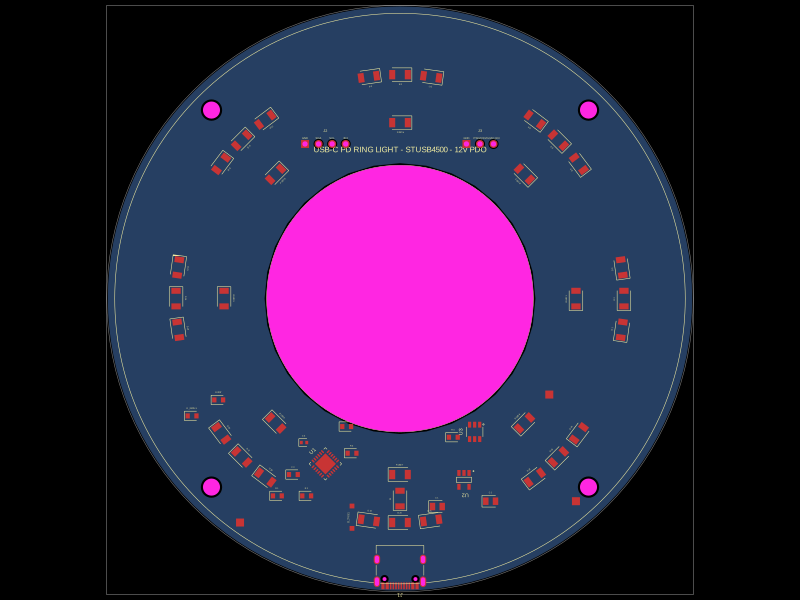
Schematic
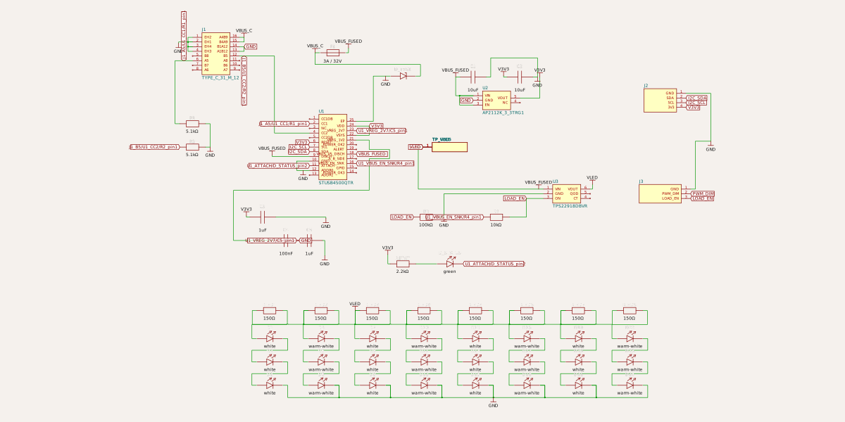
import { UsbC } from "./imports/UsbC"
import { STUSB4500QTR } from "./imports/STUSB4500QTR"
import { TPS22918DBVR } from "./imports/TPS22918DBVR"
import { AP2112K_3_3TRG1 } from "./imports/AP2112K_3_3TRG1"

const OUTER_RADIUS = 55
const INNER_RADIUS = 25
const LED_RADIUS = 42
const RESISTOR_RADIUS = 33

const circlePoints = (radius: number, count = 128) =>
  Array.from({ length: count }, (_, i) => {
    const theta = (2 * Math.PI * i) / count
    return {
      x: Number((Math.cos(theta) * radius).toFixed(3)),
      y: Number((Math.sin(theta) * radius).toFixed(3)),
    }
  })

const polar = (radius: number, degrees: number) => {
  const theta = (degrees * Math.PI) / 180
  return {
    x: Number((Math.cos(theta) * radius).toFixed(3)),
    y: Number((Math.sin(theta) * radius).toFixed(3)),
  }
}

const TestPad = (props: any) => (
  <chip
    {...props}
    pinLabels={{ pin1: "pin1" }}
    footprint={
      <footprint>
        <smtpad
          portHints={["pin1", "1"]}
          pcbX="0mm"
          pcbY="0mm"
          width="1.5mm"
          height="1.5mm"
          shape="rect"
        />
      </footprint>
    }
  />
)

const LedString = ({ stringIndex, startLedIndex }: any) => {
  const centerAngle = stringIndex * 45
  const ledAngles = [centerAngle - 8, centerAngle, centerAngle + 8]
  const resistorPoint = polar(RESISTOR_RADIUS, centerAngle)
  const resistorName = `RLED${stringIndex + 1}`

  return (
    <>
      <resistor
        name={resistorName}
        resistance="150"
        footprint="1206"
        pcbX={resistorPoint.x}
        pcbY={resistorPoint.y}
        pcbRotation={centerAngle + 90}
        schX={stringIndex * 2.2 - 7.7}
        schY={-7}
      />
      {ledAngles.map((angle: number, i: number) => {
        const p = polar(LED_RADIUS, angle)
        return (
          <led
            key={angle}
            name={`D${startLedIndex + i}`}
            color={stringIndex % 2 === 0 ? "white" : "warm-white"}
            footprint="1206"
            pcbX={p.x}
            pcbY={p.y}
            pcbRotation={angle + 90}
            schX={stringIndex * 2.2 - 7.7}
            schY={-8.2 - i}
          />
        )
      })}
      <trace from={`.${resistorName} .pin1`} to="net.VLED" />
      <trace from={`.${resistorName} .pin2`} to={`.D${startLedIndex} .anode`} />
      <trace from={`.D${startLedIndex} .cathode`} to={`.D${startLedIndex + 1} .anode`} />
      <trace from={`.D${startLedIndex + 1} .cathode`} to={`.D${startLedIndex + 2} .anode`} />
      <trace from={`.D${startLedIndex + 2} .cathode`} to="net.GND" />
    </>
  )
}

export default () => (
  <board outline={circlePoints(OUTER_RADIUS)}>
    <cutout shape="circle" radius={INNER_RADIUS} pcbX={0} pcbY={0} />
    <silkscreencircle pcbX={0} pcbY={0} radius={INNER_RADIUS} />
    <silkscreencircle pcbX={0} pcbY={0} radius={OUTER_RADIUS - 1.5} />
    <silkscreentext
      pcbX={0}
      pcbY={28}
      text="USB-C PD RING LIGHT - STUSB4500 - 12V PDO"
      fontSize={1.5}
      anchorAlignment="center"
    />

    <UsbC name="J1" pcbX={0} pcbY={-51.7} pcbRotation={180} schX={-10} schY={4} />
    <fuse
      name="F1"
      currentRating="3A"
      voltageRating="32V"
      footprint="1206"
      pcbX={0}
      pcbY={-37.5}
      pcbRotation={90}
      schX={-5}
      schY={4}
    />
    <diode
      zener
      name="D_TVS1"
      footprint="sod123"
      pcbX={-10}
      pcbY={-41}
      pcbRotation={90}
      schX={-2}
      schY={3}
    />

    <STUSB4500QTR name="U1" pcbX={-14} pcbY={-31} pcbRotation={45} schX={-5} schY={0} />
    <AP2112K_3_3TRG1 name="U2" pcbX={12} pcbY={-34} pcbRotation={180} schX={2} schY={2} />
    <TPS22918DBVR name="U3" pcbX={14} pcbY={-25} pcbRotation={90} schX={5} schY={-2} />

    <capacitor name="C1" capacitance="10uF" footprint="0805" pcbX={7} pcbY={-39} schX={1} schY={3} />
    <capacitor name="C2" capacitance="10uF" footprint="0805" pcbX={17} pcbY={-38} schX={3} schY={3} />
    <capacitor name="C3" capacitance="1uF" footprint="0603" pcbX={-20} pcbY={-33} schX={-8} schY={-3} />
    <capacitor name="C4" capacitance="100nF" footprint="0402" pcbX={-18} pcbY={-27} schX={-7} schY={-4} />
    <capacitor name="C5" capacitance="1uF" footprint="0603" pcbX={-10} pcbY={-24} schX={-6} schY={-4} />

    <resistor name="R1" resistance="5.1k" footprint="0603" pcbX={-23} pcbY={-37} schX={-11} schY={1} />
    <resistor name="R2" resistance="5.1k" footprint="0603" pcbX={-17.5} pcbY={-37} schX={-11} schY={0} />
    <resistor name="R3" resistance="100k" footprint="0603" pcbX={-9} pcbY={-29} schX={-1} schY={-3} />
    <resistor name="R4" resistance="10k" footprint="0603" pcbX={10} pcbY={-26} schX={2} schY={-3} />
    <resistor name="RSTAT" resistance="2.2k" footprint="0603" pcbX={-34} pcbY={-19} schX={-2} schY={-5} />
    <led name="D_STATUS" color="green" footprint="0603" pcbX={-39} pcbY={-22} schX={0} schY={-5} />

    <pinheader
      name="J2"
      pinCount={4}
      pinLabels={["GND", "SDA", "SCL", "3V3"]}
      footprint="pinrow4"
      pcbX={-14}
      pcbY={29}
      pcbRotation={0}
      schX={9}
      schY={2}
    />
    <pinheader
      name="J3"
      pinCount={3}
      pinLabels={["GND", "PWM_DIM", "LOAD_EN"]}
      footprint="pinrow3"
      pcbX={15}
      pcbY={29}
      pcbRotation={0}
      schX={9}
      schY={-2}
    />

    {Array.from({ length: 8 }, (_, i) => (
      <LedString key={i} stringIndex={i} startLedIndex={i * 3 + 1} />
    ))}

    {[45, 135, 225, 315].map((angle) => {
      const p = polar(50, angle)
      return <hole key={angle} diameter="3.2mm" pcbX={p.x} pcbY={p.y} />
    })}

    <TestPad
      name="TP_VBUS"
      pcbX={-30}
      pcbY={-42}
    />
    <TestPad
      name="TP_VLED"
      pcbX={28}
      pcbY={-18}
    />
    <TestPad
      name="TP_GND"
      pcbX={33}
      pcbY={-38}
    />

    <trace from=".J1 .A4B9" to="net.VBUS_C" width="0.35mm" />
    <trace from=".J1 .B4A9" to="net.VBUS_C" width="0.35mm" />
    <trace from=".J1 .A1B12" to="net.GND" />
    <trace from=".J1 .B1A12" to="net.GND" />
    <trace from=".J1 .EH1" to="net.GND" />
    <trace from=".J1 .EH2" to="net.GND" />
    <trace from=".J1 .EH3" to="net.GND" />
    <trace from=".J1 .EH4" to="net.GND" />
    <trace from=".J1 .A5" to=".U1 .CC1" />
    <trace from=".J1 .B5" to=".U1 .CC2" />

    <trace from=".F1 .pin1" to="net.VBUS_C" width="0.45mm" />
    <trace from=".F1 .pin2" to="net.VBUS_FUSED" width="0.45mm" />
    <trace from=".D_TVS1 .anode" to="net.GND" />
    <trace from=".D_TVS1 .cathode" to="net.VBUS_C" />
    <trace from=".TP_VBUS .pin1" to="net.VBUS_FUSED" />

    <trace from=".U1 .VBUS_VS_DISCH" to="net.VBUS_FUSED" />
    <trace from=".U1 .DISCH" to="net.VBUS_FUSED" />
    <trace from=".U1 .VSYS" to="net.V3V3" />
    <trace from=".U1 .VDD" to="net.V3V3" />
    <trace from=".U1 .VREG_1V2" to=".C4 .pin1" />
    <trace from=".U1 .VREG_2V7" to=".C5 .pin1" />
    <trace from=".U1 .GND" to="net.GND" />
    <trace from=".U1 .EP" to="net.GND" />
    <trace from=".U1 .ADDR0" to="net.GND" />
    <trace from=".U1 .RESET" to="net.V3V3" />
    <trace from=".U1 .SDA" to="net.I2C_SDA" />
    <trace from=".U1 .SCL" to="net.I2C_SCL" />
    <trace from=".U1 .VBUS_EN_SNK" to=".R4 .pin1" />
    <trace from=".R4 .pin2" to="net.LOAD_EN" />

    <trace from=".U2 .VIN" to="net.VBUS_FUSED" />
    <trace from=".U2 .EN" to="net.VBUS_FUSED" />
    <trace from=".U2 .VOUT" to="net.V3V3" />
    <trace from=".U2 .GND" to="net.GND" />
    <trace from=".C1 .pin1" to="net.VBUS_FUSED" />
    <trace from=".C1 .pin2" to="net.GND" />
    <trace from=".C2 .pin1" to="net.V3V3" />
    <trace from=".C2 .pin2" to="net.GND" />
    <trace from=".C3 .pin1" to="net.V3V3" />
    <trace from=".C3 .pin2" to="net.GND" />
    <trace from=".C4 .pin2" to="net.GND" />
    <trace from=".C5 .pin2" to="net.GND" />

    <trace from=".U3 .VIN" to="net.VBUS_FUSED" width="0.45mm" />
    <trace from=".U3 .VOUT" to="net.VLED" width="0.45mm" />
    <trace from=".U3 .ON" to="net.LOAD_EN" />
    <trace from=".U3 .GND" to="net.GND" />
    <trace from=".TP_VLED .pin1" to="net.VLED" />
    <trace from=".TP_GND .pin1" to="net.GND" />

    <trace from=".R1 .pin1" to=".J1 .A5" />
    <trace from=".R1 .pin2" to="net.GND" />
    <trace from=".R2 .pin1" to=".J1 .B5" />
    <trace from=".R2 .pin2" to="net.GND" />
    <trace from=".R3 .pin1" to="net.LOAD_EN" />
    <trace from=".R3 .pin2" to="net.GND" />

    <trace from=".RSTAT .pin1" to="net.V3V3" />
    <trace from=".RSTAT .pin2" to=".D_STATUS .anode" />
    <trace from=".D_STATUS .cathode" to=".U1 .ATTACH" />

    <trace from=".J2 .GND" to="net.GND" />
    <trace from=".J2 .SDA" to="net.I2C_SDA" />
    <trace from=".J2 .SCL" to="net.I2C_SCL" />
    <trace from=".J2 .3V3" to="net.V3V3" />
    <trace from=".J3 .GND" to="net.GND" />
    <trace from=".J3 .PWM_DIM" to="net.PWM_DIM" />
    <trace from=".J3 .LOAD_EN" to="net.LOAD_EN" />

    <copperpour connectsTo="net.GND" layer="bottom" cutoutMargin="0.4mm" />
  </board>
)