imrishabh18/pcbgolf
These code snippets define detailed PCB footprints for various SMD components, through-hole connectors, and chips, specifying pad locations, shapes, silkscreen outlines, and mechanical outlines for physical placement on a circuit board.
- Version
- 1.4.3
- License
- unset
- Stars
- 0
tests/drc-regressions.test.ts
import { describe, expect, test } from 'bun:test'
import { checkTracesAreContiguous, checkPadTraceClearance, checkViaPadClearance, checkPadPadClearance } from '@tscircuit/checks'
const pad = (id: string, x: number, y=0): any => ({type:'pcb_smtpad', pcb_smtpad_id:id, pcb_port_id:`port_${id}`, shape:'rect', x,y,width:0.6,height:0.6,layer:'top'})
const wire=(x:number,y=0,layer='top'):any=>({route_type:'wire',x,y,layer,width:0.2})
const trace=(id:string, route:any[]):any=>({type:'pcb_trace',pcb_trace_id:`trace_${id}`,source_trace_id:'net_trace',route})
const via=(id:string,x:number,layers=['top','inner1','bottom']):any=>({type:'pcb_via',pcb_via_id:id,x,y:0,outer_diameter:0.5,hole_diameter:0.2,layers})
function fixture(parts:any[]) {
 const pads=parts.filter(x=>x.type==='pcb_smtpad')
 return [ {type:'source_trace',source_trace_id:'net_trace',connected_source_port_ids:pads.map(p=>`source_${p.pcb_smtpad_id}`)},
 ...pads.map(p=>({type:'pcb_port',pcb_port_id:p.pcb_port_id,source_port_id:`source_${p.pcb_smtpad_id}`,x:p.x,y:p.y,layers:[p.layer]})),...parts] as any
}
const errors=(parts:any[])=>checkTracesAreContiguous(fixture(parts))
const ring=(x1:number,y1:number,x2:number,y2:number)=>({vertices:[{x:x1,y:y1},{x:x2,y:y1},{x:x2,y:y2},{x:x1,y:y2}]})
const plane:any={type:'pcb_copper_pour',pcb_copper_pour_id:'plane',shape:'brep',layer:'inner1',brep_shape:{outer_ring:ring(-1,-1,6,1),inner_rings:[]}}
describe('physical connectivity',()=>{
 test('joins branches through actual via barrels across layers',()=>{
  const parts=[pad('a',0),{...pad('b',5),layer:'bottom'},trace('a',[wire(0),wire(2)]),trace('b',[wire(2,0,'bottom'),wire(5,0,'bottom')]),via('v',2)]
  expect(errors(parts)).toHaveLength(0)
  expect(errors(parts.filter(p=>p.type!=='pcb_via')).length).toBeGreaterThan(0)
  expect(errors(parts.map(p=>p.type==='pcb_via'?{...p,layers:['bottom']}:p)).length).toBeGreaterThan(0)
 })
 test('does not trust logical net identity or spoofed endpoint IDs across a gap',()=>{
  const parts=[pad('a',0),pad('b',5),trace('a',[wire(0),{...wire(1),end_pcb_port_id:'port_b'}]),trace('b',[wire(4),wire(5)])]
  expect(errors(parts).length).toBeGreaterThan(0)
 })
 test('recognizes intermediate pad contacts and copper-width branch contact',()=>{
  const parts=[pad('a',0),pad('b',3),pad('c',1,1),trace('a',[wire(-1),wire(4)]),trace('b',[wire(1,0.19),wire(1,1)])]
  expect(errors(parts)).toHaveLength(0)
  expect(errors(parts.map(p=>p.pcb_trace_id==='trace_b'?trace('b',[wire(1,0.21),wire(1,1)]):p)).length).toBeGreaterThan(0)
 })
 test('ground plane joins vias, but absent planes, voids and wrong layers do not',()=>{
  const parts=[pad('a',0),pad('b',5),trace('a',[wire(0),wire(1)]),trace('b',[wire(4),wire(5)]),via('v1',1),via('v2',4)]
  expect(errors([...parts,plane])).toHaveLength(0)
  expect(errors(parts).length).toBeGreaterThan(0)
  expect(errors([...parts,{...plane,layer:'inner2'}]).length).toBeGreaterThan(0)
  expect(errors([...parts,{...plane,brep_shape:{...plane.brep_shape,inner_rings:[ring(3.5,-0.5,4.5,0.5)]}}]).length).toBeGreaterThan(0)
 })
 test('recognizes a via-only route only when a physical barrel exists',()=>{
  const parts=[pad('a',0),pad('b',5),trace('barrel',[wire(2,0,'bottom'),{route_type:'via',x:2,y:0,from_layer:'bottom',to_layer:'top',via_diameter:0.5,via_hole_diameter:0.2},wire(2)]),trace('a',[wire(0),wire(2)]),trace('b',[wire(2),wire(5)]),via('v',2)]
  expect(errors(parts)).toHaveLength(0)
  expect(errors(parts.filter(p=>p.type!=='pcb_via')).length).toBeGreaterThan(0)
 })
})
describe('clearance geometry and rules',()=>{
 const rounded={...pad('a',0),width:2,height:2,corner_radius:0.5}
 test('uses exact rounded corners for pad-to-trace clearance, retaining real violations',()=>{
  const t=trace('other',[wire(1.3,1.3),wire(2,1.3)])
  expect(checkPadTraceClearance([rounded,t],{minClearance:0.5})).toHaveLength(0)
  expect(checkPadTraceClearance([{...rounded,corner_radius:0},t],{minClearance:0.5})).toHaveLength(1)
  expect(checkPadTraceClearance([rounded,trace('other',[wire(1.2,1.2),wire(2,1.2)])],{minClearance:0.5})).toHaveLength(1)
 })
 test('uses exact rounded corners for via clearance',()=>{
  expect(checkViaPadClearance([rounded,{...via('v',1.3),y:1.3,outer_diameter:0.2}],{minClearance:0.5})).toHaveLength(0)
  expect(checkViaPadClearance([rounded,{...via('v',1.2),y:1.2,outer_diameter:0.2}],{minClearance:0.5})).toHaveLength(1)
 })
 test('keeps stricter SMT pad-to-pad spacing distinct from via copper clearance',()=>{
  const board:any={type:'pcb_board',pcb_board_id:'board',min_pad_edge_to_pad_edge_clearance:0.15,min_trace_to_pad_edge_clearance:0.1}
  const rect={...rounded,corner_radius:0}
  expect(checkViaPadClearance([board,rect,{...via('v',1.225),outer_diameter:0.2}])).toHaveLength(0)
  expect(checkViaPadClearance([board,rect,{...via('v',1.175),outer_diameter:0.2}])).toHaveLength(1)
  expect(checkPadPadClearance([board,rect,{...pad('b',1.225),shape:'circle',radius:0.1}])).toHaveLength(1)
 })
})
Related Packages
 More from this authorimrishabh18/C12084Generated from JLCPCB part number C12084
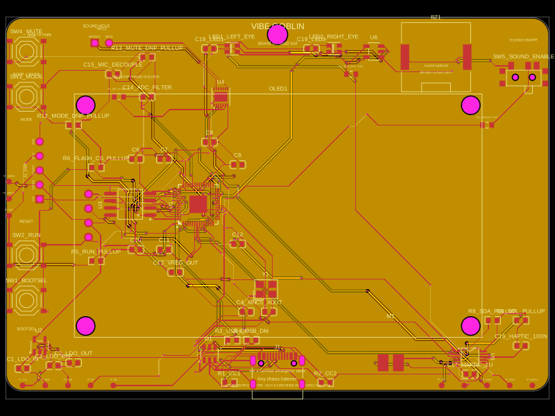 Similar packageAnasSarkiz/vibe_GoblinThese code snippets define various physical electronic components such as ICs, connectors, sensors, LEDs, and chips, specifying their pin layouts, footprint pads, silkscreen markings, courtyard outlines, and 3D CAD models for placement on PCB boards.
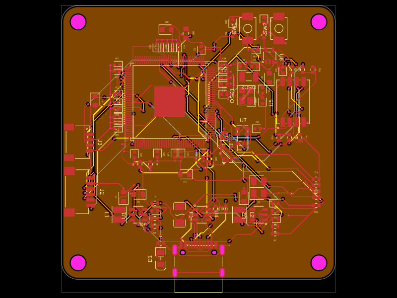 Discover something newtechmannih/trellis-coreThis code defines a detailed electronic hardware schematic and PCB layout for a Linux System-on-Module, incorporating components such as oscillators, power regulators, USB-C connectors, connectors, LEDs, resistors, capacitors, inductors, and integrated circuits, with precise physical footprint and 3D models.