imrishabh18/pcbgolf
This code defines detailed PCB footprints for various electronic components (such as resistors, capacitors, connectors, ICs, LEDs, and via/hole patterns), as well as associated metadata (pin mappings, CAD models, labels) for a circuit design, enabling precise rendering and integration into a PCB layout in a React-based schematic editor.
- Version
- 1.4.1
- License
- unset
- Stars
- 0
imports/SI7101DN_T1_GE3.tsx
// Imported with tsci import --jlcpcb --use-exact-footprint C142572
export const C142572CadModel = {
        objUrl: "https://modelcdn.tscircuit.com/easyeda_models/assets/C142572.obj?uuid=24f5b394c4324896b68f4e92d9cfb751",
        stepUrl: "https://modelcdn.tscircuit.com/easyeda_models/assets/C142572.step?uuid=24f5b394c4324896b68f4e92d9cfb751",
        pcbRotationOffset: 0,
        modelOriginPosition: { x: 0.00013970000009067007, y: -0.000038099999983387534, z: -0.29 },
      }

import type { ChipProps } from "@tscircuit/props"

const pinLabels = {
  pin1: ["S3"],
  pin2: ["S2"],
  pin3: ["S1"],
  pin4: ["G"],
  pin5: ["D4"],
  pin6: ["D3"],
  pin7: ["D2"],
  pin8: ["D1"]
} as const

export const SI7101DN_T1_GE3 = (props: ChipProps<typeof pinLabels>) => {
  return (
    <chip
      pinLabels={pinLabels}
      supplierPartNumbers={{
  "jlcpcb": [
    "C142572"
  ]
}}
      manufacturerPartNumber="SI7101DN-T1-GE3"
      footprint={<footprint>
        <smtpad portHints={["pin8"]} pcbX="0mm" pcbY="0.399923mm" width="2.5999948mm" height="2.1999956mm" shape="rect" />
<smtpad portHints={["pin8"]} pcbX="-0.975106mm" pcbY="1.499997mm" width="0.4500118mm" height="0.700024mm" shape="rect" />
<smtpad portHints={["pin7"]} pcbX="-0.32512mm" pcbY="1.499997mm" width="0.4500118mm" height="0.700024mm" shape="rect" />
<smtpad portHints={["pin6"]} pcbX="0.324866mm" pcbY="1.499997mm" width="0.4500118mm" height="0.700024mm" shape="rect" />
<smtpad portHints={["pin5"]} pcbX="0.974852mm" pcbY="1.499997mm" width="0.4500118mm" height="0.700024mm" shape="rect" />
<smtpad portHints={["pin4"]} pcbX="0.974852mm" pcbY="-1.499997mm" width="0.4500118mm" height="0.700024mm" shape="rect" />
<smtpad portHints={["pin3"]} pcbX="0.324866mm" pcbY="-1.499997mm" width="0.4500118mm" height="0.700024mm" shape="rect" />
<smtpad portHints={["pin2"]} pcbX="-0.32512mm" pcbY="-1.499997mm" width="0.4500118mm" height="0.700024mm" shape="rect" />
<smtpad portHints={["pin1"]} pcbX="-0.975106mm" pcbY="-1.499997mm" width="0.4500118mm" height="0.700024mm" shape="rect" />
<silkscreenpath route={[{"x":1.549780999999939,"y":1.5500858000000335},{"x":1.549780999999939,"y":-1.549730199999999}]} />
<silkscreenpath route={[{"x":-1.5500349999999798,"y":-1.549730199999999},{"x":-1.5500349999999798,"y":1.5500858000000335}]} />
<silkscreencircle pcbX="-1.560068mm" pcbY="-2.000123mm" radius="0.127mm" />
<silkscreentext text="{NAME}" pcbX="-0.014732mm" pcbY="2.847977mm" anchorAlignment="center" fontSize="1mm" />
<courtyardoutline outline={[{"x":-1.9284320000001571,"y":2.0979770000000144},{"x":1.8989679999998543,"y":2.0979770000000144},{"x":1.8989679999998543,"y":-2.3898229999999785},{"x":-1.9284320000001571,"y":-2.3898229999999785},{"x":-1.9284320000001571,"y":2.0979770000000144}]} />
      </footprint>}
      cadModel={C142572CadModel}
      {...props}
    />
  )
}
Related Packages
 More from this authorimrishabh18/C12084Generated from JLCPCB part number C12084
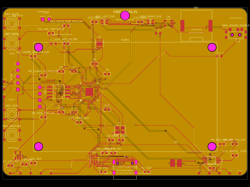 Similar packageAnasSarkiz/vibe_GoblinThese code snippets define various physical electronic components such as ICs, connectors, sensors, LEDs, and chips, specifying their pin layouts, footprint pads, silkscreen markings, courtyard outlines, and 3D CAD models for placement on PCB boards.
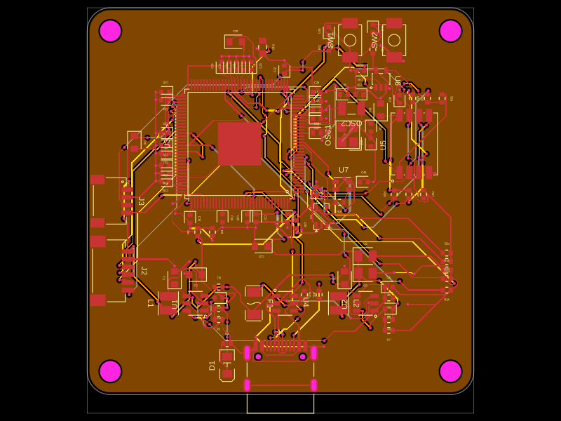 Discover something newtechmannih/trellis-coreThis code defines a detailed electronic hardware schematic and PCB layout for a Linux System-on-Module, incorporating components such as oscillators, power regulators, USB-C connectors, connectors, LEDs, resistors, capacitors, inductors, and integrated circuits, with precise physical footprint and 3D models.