imrishabh18/motor-driver-breakout
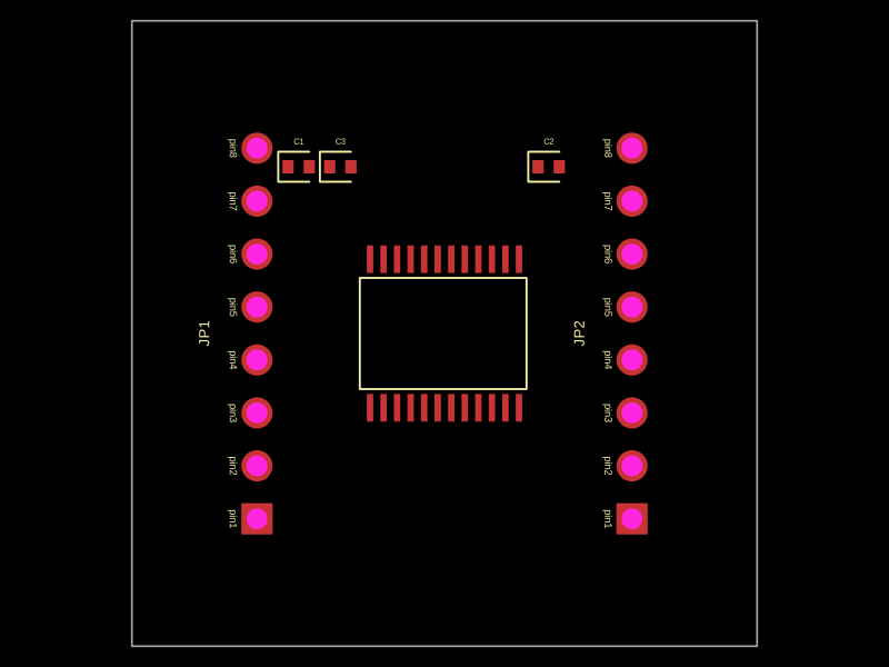
"A 30x30mm TB6612FNG motor driver board with dual 8-pin headers and bypass capacitors for motor control and power regulation" This summary captures the key physical characteristics: - Uses TB6612FNG motor driver chip - 30x30mm board size - Dual 8-pin headers (JP1 and JP2) - Includes decoupling capacitors (C1, C2, C3) - Purpose is motor control and power management
Usage: Based on the provided code, here's a concise guide to importing and using the motor driver breakout component: 1. Import the component: ```tsx import MotorDriverBreakout from "@tsci/imrishabh18.motor-driver-breakout" ``` 2. Use the component in a board layout: ```tsx <board width="30mm" height="30mm"> <MotorDriverBreakout /> {/* Other components and traces can be added as needed */} </board> ``` Key points: - The component includes a motor driver, pin headers, and supporting capacitors - It has predefined traces and component placements - Optional manual edits can be included via a `manualEdits` prop - The component uses an autorouter for trace routing
- Version
- 0.0.1
- License
- MIT
- Stars
- 5
index.tsx
PCB
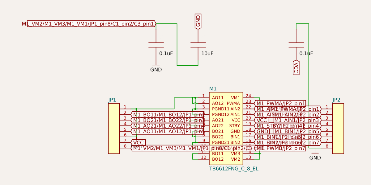
Schematic
import { TB6612FNG_C_8_EL as MotorDriver } from "@tsci/imrishabh18.TB6612FNG"
import manaulEdits from "./manual-edits.json"

export default () => {
  return (
    <board width="25mm" height="25mm" autorouter="auto-cloud" manualEdits={manaulEdits}>
      <MotorDriver name="M1" />
      <pinheader
        name="JP1"
        pinCount={8}
        pcbX={-9}
        pcbRotation={90}
        schX={-4}
        footprint="pinrow8"
      />
      <pinheader
        name="JP2"
        pinCount={8}
        pcbX={9}
        pcbRotation={90}
        schX={4}
        schRotation={180}
        footprint="pinrow8"
        facingDirection="left"
      />
      <capacitor
        name="C1"
        capacitance="0.1uF"
        pcbX={-7}
        pcbY={8}
        schX={-2.5}
        schY={3}
        footprint="0402"
        schRotation={90}
      />
      <capacitor
        name="C3"
        capacitance="10uF"
        pcbX={-5}
        pcbY={8}
        schX={-1}
        schY={3}
        footprint="0402"
        schRotation={90}
      />
      <capacitor
        name="C2"
        capacitance="0.1uF"
        pcbX={5}
        pcbY={8}
        schX={2.5}
        schY={3}
        footprint="0402"
        schRotation={90}
      />

      <trace from=".JP1 > .pin8" to=".C1 > .neg" />
      <trace from=".JP1 > .pin8" to=".C3 > .pos" />
      <trace from=".JP1 > .pin8" to=".M1 > .pin24" />
      <trace from=".JP1 > .pin8" to=".M1 > .pin14" />
      <trace from=".JP1 > .pin7" to="net.VCC" />
      <trace from=".JP1 > .pin6" to="net.GND" />
      <trace from=".JP1 > .pin5" to=".M1 > .pin1" />
      <trace from=".JP1 > .pin5" to=".M1 > .pin2" />
      <trace from=".JP1 > .pin4" to=".M1 > .pin5" />
      <trace from=".JP1 > .pin4" to=".M1 > .pin6" />
      <trace from=".JP1 > .pin3" to=".M1 > .pin7" />
      <trace from=".JP1 > .pin3" to=".M1 > .pin8" />
      <trace from=".JP1 > .pin2" to=".M1 > .pin11" />
      <trace from=".JP1 > .pin2" to=".M1 > .pin12" />
      <trace from=".JP1 > .pin1" to="net.GND" />

      <trace from=".JP2 > .pin8" to="net.GND" />
      <trace from=".JP2 > .pin7" to=".M1 > .pin15" />
      <trace from=".JP2 > .pin6" to=".M1 > .pin16" />
      <trace from=".JP2 > .pin5" to=".M1 > .pin17" />
      <trace from=".JP2 > .pin4" to=".M1 > .pin19" />
      <trace from=".JP2 > .pin3" to=".M1 > .pin21" />
      <trace from=".JP2 > .pin2" to=".M1 > .pin22" />
      <trace from=".JP2 > .pin1" to=".M1 > .pin23" />

      <trace from=".C1 > .pos" to="net.GND" />
      <trace from=".C3 > .neg" to="net.GND" />
      <trace from=".C1 > .neg" to=".M1 > .pin24" />
      <trace from=".C3 > .pos" to=".M1 > .pin24" />
      <trace from=".C1 > .neg" to=".M1 > .pin14" />
      <trace from=".C3 > .pos" to=".M1 > .pin14" />
      <trace from=".C1 > .neg" to=".M1 > .pin13" />
      <trace from=".C3 > .pos" to=".M1 > .pin13" />

      <trace from=".C2 > .pos" to="net.VCC" />
      <trace from=".C2 > .neg" to="net.GND" />

      <trace from=".M1 > .pin18" to="net.GND" />
      <trace from=".M1 > .pin20" to="net.VCC" />
      <trace from=".M1 > .pin3" to="net.GND" />
      <trace from=".M1 > .pin4" to="net.GND" />
      <trace from=".M1 > .pin9" to="net.GND" />
      <trace from=".M1 > .pin10" to="net.GND" />
    </board>
  )
}
Related Packages
 More from this authorimrishabh18/boost-converterThis code defines a PCB schematic and 3D model layout focusing on a power conversion circuit with components like USB-C connector, MT3608 step-up regulator, inductor, diode, input/output capacitors, and resistors arranged on a double-layer PCB.
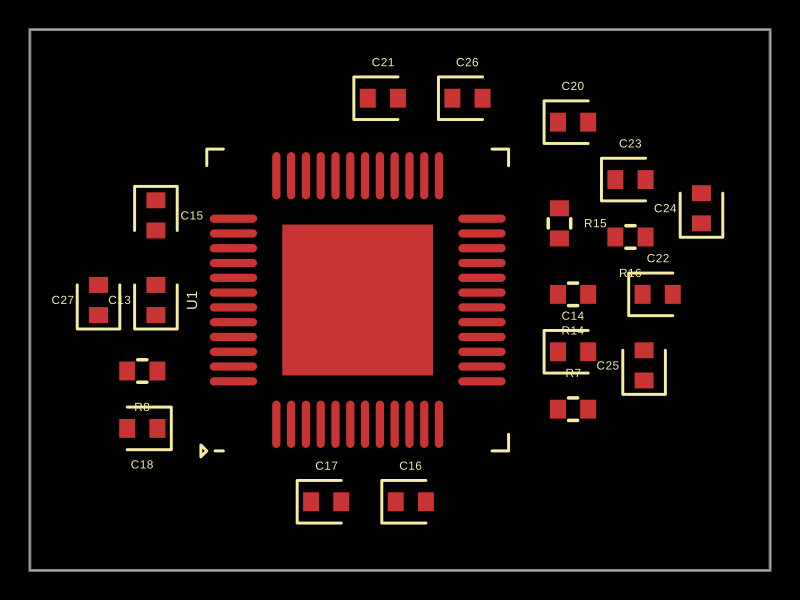 Similar packageMustafaMulla29/ti-chipThis code models a hardware circuit for a motor driver using a DRV83053QPHPQ1 integrated circuit, with power supply bypass capacitors, charge-pump capacitors, resistors, and filters, representing the physical connections and key components in a motor control power stage.
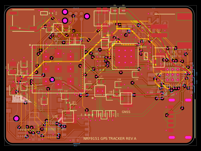 Discover something newpixalynx/nrf9151-gps-trackerA compact 44×32 mm, 4-layer nRF9151 LTE-M/NB-IoT/GNSS tracker PCB with nPM1300 LiPo/USB-C power, nano-SIM/eSIM switching, nRF7002 Wi‑Fi scanning, accelerometer, antennas, buzzer, LEDs, SOS button, and SWD/debug connectors.