imrishabh18/motor-driver-breakout
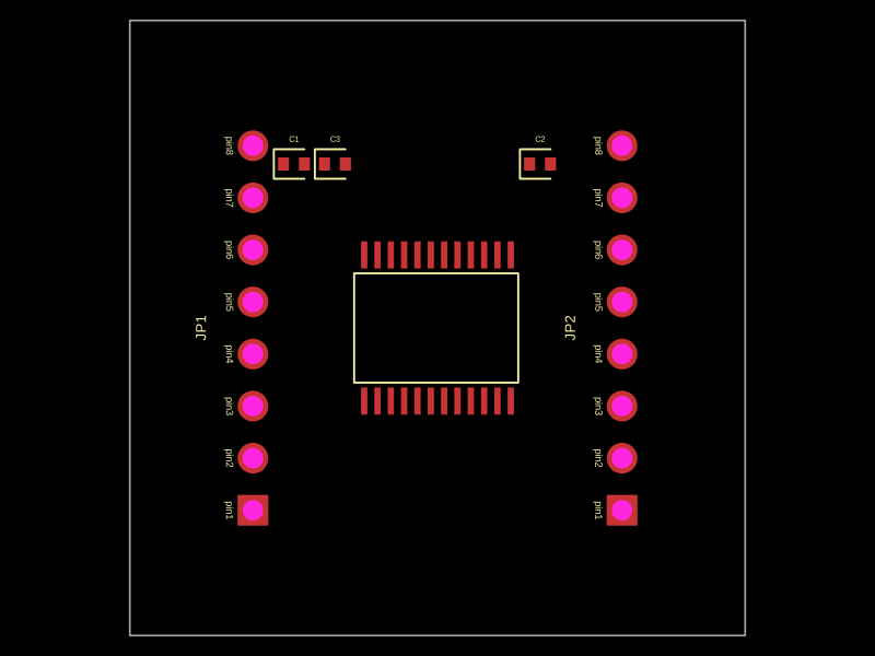
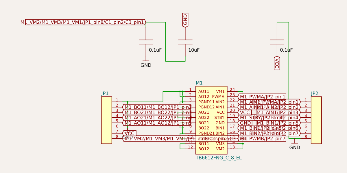
"A 30x30mm TB6612FNG motor driver board with dual 8-pin headers and bypass capacitors for motor control and power regulation" This summary captures the key physical characteristics: - Uses TB6612FNG motor driver chip - 30x30mm board size - Dual 8-pin headers (JP1 and JP2) - Includes decoupling capacitors (C1, C2, C3) - Purpose is motor control and power management
Usage: Based on the provided code, here's a concise guide to importing and using the motor driver breakout component: 1. Import the component: ```tsx import MotorDriverBreakout from "@tsci/imrishabh18.motor-driver-breakout" ``` 2. Use the component in a board layout: ```tsx <board width="30mm" height="30mm"> <MotorDriverBreakout /> {/* Other components and traces can be added as needed */} </board> ``` Key points: - The component includes a motor driver, pin headers, and supporting capacitors - It has predefined traces and component placements - Optional manual edits can be included via a `manualEdits` prop - The component uses an autorouter for trace routing
- Version
- 0.0.1
- License
- MIT
- Stars
- 5
dist/pcb.svg
PCB
Schematic
<svg xmlns="http://www.w3.org/2000/svg" width="800" height="600" data-software-used-string="@tscircuit/core@0.0.941"><style></style><rect class="boundary" x="0" y="0" fill="#000" width="800" height="600" data-type="pcb_background" data-pcb-layer="global"/><rect class="pcb-boundary" fill="none" stroke="#fff" stroke-width="0.3" x="118.75" y="18.75" width="562.5" height="562.5" data-type="pcb_boundary" data-pcb-layer="global"/><path class="pcb-board" d="M 118.75 581.25 L 681.25 581.25 L 681.25 18.75 L 118.75 18.75 Z" fill="none" stroke="rgba(255, 255, 255, 0.5)" stroke-width="1.875" data-type="pcb_board" data-pcb-layer="board"/><rect class="pcb-pad" fill="rgb(200, 52, 52)" x="330.08030874999935" y="354.3767962499978" width="5.775007499999999" height="24.8250075" data-type="pcb_smtpad" data-pcb-layer="top"/><rect class="pcb-pad" fill="rgb(200, 52, 52)" x="342.26754624999745" y="354.3767962499978" width="5.775007499999999" height="24.8250075" data-type="pcb_smtpad" data-pcb-layer="top"/><rect class="pcb-pad" fill="rgb(200, 52, 52)" x="354.4547837499999" y="354.3767962499978" width="5.775007499999999" height="24.8250075" data-type="pcb_smtpad" data-pcb-layer="top"/><rect class="pcb-pad" fill="rgb(200, 52, 52)" x="366.642021249998" y="354.3767962499978" width="5.775007499999999" height="24.8250075" data-type="pcb_smtpad" data-pcb-layer="top"/><rect class="pcb-pad" fill="rgb(200, 52, 52)" x="378.8292587500003" y="354.3767962499978" width="5.775007499999999" height="24.8250075" data-type="pcb_smtpad" data-pcb-layer="top"/><rect class="pcb-pad" fill="rgb(200, 52, 52)" x="391.02125874999916" y="354.3767962499978" width="5.775007499999999" height="24.8250075" data-type="pcb_smtpad" data-pcb-layer="top"/><rect class="pcb-pad" fill="rgb(200, 52, 52)" x="403.2084962500016" y="354.3767962499978" width="5.775007499999999" height="24.8250075" data-type="pcb_smtpad" data-pcb-layer="top"/><rect class="pcb-pad" fill="rgb(200, 52, 52)" x="415.3957337499997" y="354.3767962499978" width="5.775007499999999" height="24.8250075" data-type="pcb_smtpad" data-pcb-layer="top"/><rect class="pcb-pad" fill="rgb(200, 52, 52)" x="427.5829712499999" y="354.3767962499978" width="5.775007499999999" height="24.8250075" data-type="pcb_smtpad" data-pcb-layer="top"/><rect class="pcb-pad" fill="rgb(200, 52, 52)" x="439.7702087500001" y="354.3767962499978" width="5.775007499999999" height="24.8250075" data-type="pcb_smtpad" data-pcb-layer="top"/><rect class="pcb-pad" fill="rgb(200, 52, 52)" x="451.9574462500004" y="354.3767962499978" width="5.775007499999999" height="24.8250075" data-type="pcb_smtpad" data-pcb-layer="top"/><rect class="pcb-pad" fill="rgb(200, 52, 52)" x="464.1446837499985" y="354.3767962499978" width="5.775007499999999" height="24.8250075" data-type="pcb_smtpad" data-pcb-layer="top"/><rect class="pcb-pad" fill="rgb(200, 52, 52)" x="330.08030874999935" y="220.79819625000005" width="5.775007499999999" height="24.8250075" data-type="pcb_smtpad" data-pcb-layer="top"/><rect class="pcb-pad" fill="rgb(200, 52, 52)" x="342.26754624999745" y="220.79819625000005" width="5.775007499999999" height="24.8250075" data-type="pcb_smtpad" data-pcb-layer="top"/><rect class="pcb-pad" fill="rgb(200, 52, 52)" x="354.4547837499999" y="220.79819625000005" width="5.775007499999999" height="24.8250075" data-type="pcb_smtpad" data-pcb-layer="top"/><rect class="pcb-pad" fill="rgb(200, 52, 52)" x="366.642021249998" y="220.79819625000005" width="5.775007499999999" height="24.8250075" data-type="pcb_smtpad" data-pcb-layer="top"/><rect class="pcb-pad" fill="rgb(200, 52, 52)" x="378.8292587500003" y="220.79819625000005" width="5.775007499999999" height="24.8250075" data-type="pcb_smtpad" data-pcb-layer="top"/><rect class="pcb-pad" fill="rgb(200, 52, 52)" x="391.02125874999916" y="220.79819625000005" width="5.775007499999999" height="24.8250075" data-type="pcb_smtpad" data-pcb-layer="top"/><rect class="pcb-pad" fill="rgb(200, 52, 52)" x="403.2084962500016" y="220.79819625000005" width="5.775007499999999" height="24.8250075" data-type="pcb_smtpad" data-pcb-layer="top"/><rect class="pcb-pad" fill="rgb(200, 52, 52)" x="415.3957337499997" y="220.79819625000005" width="5.775007499999999" height="24.8250075" data-type="pcb_smtpad" data-pcb-layer="top"/><rect class="pcb-pad" fill="rgb(200, 52, 52)" x="427.5829712499999" y="220.79819625000005" width="5.775007499999999" height="24.8250075" data-type="pcb_smtpad" data-pcb-layer="top"/><rect class="pcb-pad" fill="rgb(200, 52, 52)" x="439.7702087500001" y="220.79819625000005" width="5.775007499999999" height="24.8250075" data-type="pcb_smtpad" data-pcb-layer="top"/><rect class="pcb-pad" fill="rgb(200, 52, 52)" x="451.9574462500004" y="220.79819625000005" width="5.775007499999999" height="24.8250075" data-type="pcb_smtpad" data-pcb-layer="top"/><rect class="pcb-pad" fill="rgb(200, 52, 52)" x="464.1446837499985" y="220.79819625000005" width="5.775007499999999" height="24.8250075" data-type="pcb_smtpad" data-pcb-layer="top"/><rect class="pcb-pad" fill="rgb(200, 52, 52)" x="254.125" y="144" width="10.125" height="12" data-type="pcb_smtpad" data-pcb-layer="top"/><rect class="pcb-pad" fill="rgb(200, 52, 52)" x="273.25" y="144" width="10.125" height="12" data-type="pcb_smtpad" data-pcb-layer="top"/><rect class="pcb-pad" fill="rgb(200, 52, 52)" x="291.625" y="144" width="10.125" height="12" data-type="pcb_smtpad" data-pcb-layer="top"/><rect class="pcb-pad" fill="rgb(200, 52, 52)" x="310.75" y="144" width="10.125" height="12" data-type="pcb_smtpad" data-pcb-layer="top"/><rect class="pcb-pad" fill="rgb(200, 52, 52)" x="479.125" y="144" width="10.125" height="12" data-type="pcb_smtpad" data-pcb-layer="top"/><rect class="pcb-pad" fill="rgb(200, 52, 52)" x="498.25" y="144" width="10.125" height="12" data-type="pcb_smtpad" data-pcb-layer="top"/><path class="pcb-silkscreen pcb-silkscreen-top" d="M 323.79999999999853 249.99375000000157 L 323.79999999999853 350.0062500000006 L 473.8187499999981 350.0062500000006 L 473.8187499999981 249.99375000000157 L 323.79999999999853 249.99375000000157 Z" fill="none" stroke="#f2eda1" stroke-width="1.875" stroke-linecap="round" stroke-linejoin="round" data-pcb-component-id="pcb_component_0" data-pcb-silkscreen-path-id="pcb_silkscreen_path_0" data-type="pcb_silkscreen_path" data-pcb-layer="top"/><text x="0" y="0" dx="0" dy="0" fill="#f2eda1" font-family="Arial, sans-serif" font-size="9.375" text-anchor="middle" dominant-baseline="central" transform="matrix(-1.8369701987210297e-16,1,-1,-1.8369701987210297e-16,210.15625,466.6875)" class="pcb-silkscreen-text pcb-silkscreen-top" data-pcb-silkscreen-text-id="pcb_component_1" stroke="none" data-type="pcb_silkscreen_text" data-pcb-layer="top">pin1</text><text x="0" y="0" dx="0" dy="0" fill="#f2eda1" font-family="Arial, sans-serif" font-size="9.375" text-anchor="middle" dominant-baseline="central" transform="matrix(-1.8369701987210297e-16,1,-1,-1.8369701987210297e-16,210.15625,419.0625)" class="pcb-silkscreen-text pcb-silkscreen-top" data-pcb-silkscreen-text-id="pcb_component_1" stroke="none" data-type="pcb_silkscreen_text" data-pcb-layer="top">pin2</text><text x="0" y="0" dx="0" dy="0" fill="#f2eda1" font-family="Arial, sans-serif" font-size="9.375" text-anchor="middle" dominant-baseline="central" transform="matrix(-1.8369701987210297e-16,1,-1,-1.8369701987210297e-16,210.15625,371.4375)" class="pcb-silkscreen-text pcb-silkscreen-top" data-pcb-silkscreen-text-id="pcb_component_1" stroke="none" data-type="pcb_silkscreen_text" data-pcb-layer="top">pin3</text><text x="0" y="0" dx="0" dy="0" fill="#f2eda1" font-family="Arial, sans-serif" font-size="9.375" text-anchor="middle" dominant-baseline="central" transform="matrix(-1.8369701987210297e-16,1,-1,-1.8369701987210297e-16,210.15625,323.8125)" class="pcb-silkscreen-text pcb-silkscreen-top" data-pcb-silkscreen-text-id="pcb_component_1" stroke="none" data-type="pcb_silkscreen_text" data-pcb-layer="top">pin4</text><text x="0" y="0" dx="0" dy="0" fill="#f2eda1" font-family="Arial, sans-serif" font-size="9.375" text-anchor="middle" dominant-baseline="central" transform="matrix(-1.8369701987210297e-16,1,-1,-1.8369701987210297e-16,210.15625,276.1875)" class="pcb-silkscreen-text pcb-silkscreen-top" data-pcb-silkscreen-text-id="pcb_component_1" stroke="none" data-type="pcb_silkscreen_text" data-pcb-layer="top">pin5</text><text x="0" y="0" dx="0" dy="0" fill="#f2eda1" font-family="Arial, sans-serif" font-size="9.375" text-anchor="middle" dominant-baseline="central" transform="matrix(-1.8369701987210297e-16,1,-1,-1.8369701987210297e-16,210.15625,228.56250000000003)" class="pcb-silkscreen-text pcb-silkscreen-top" data-pcb-silkscreen-text-id="pcb_component_1" stroke="none" data-type="pcb_silkscreen_text" data-pcb-layer="top">pin6</text><text x="0" y="0" dx="0" dy="0" fill="#f2eda1" font-family="Arial, sans-serif" font-size="9.375" text-anchor="middle" dominant-baseline="central" transform="matrix(-1.8369701987210297e-16,1,-1,-1.8369701987210297e-16,210.15625,180.9375)" class="pcb-silkscreen-text pcb-silkscreen-top" data-pcb-silkscreen-text-id="pcb_component_1" stroke="none" data-type="pcb_silkscreen_text" data-pcb-layer="top">pin7</text><text x="0" y="0" dx="0" dy="0" fill="#f2eda1" font-family="Arial, sans-serif" font-size="9.375" text-anchor="middle" dominant-baseline="central" transform="matrix(-1.8369701987210297e-16,1,-1,-1.8369701987210297e-16,210.15625,133.3125)" class="pcb-silkscreen-text pcb-silkscreen-top" data-pcb-silkscreen-text-id="pcb_component_1" stroke="none" data-type="pcb_silkscreen_text" data-pcb-layer="top">pin8</text><text x="0" y="0" dx="0" dy="0" fill="#f2eda1" font-family="Arial, sans-serif" font-size="13.125" text-anchor="middle" dominant-baseline="central" transform="matrix(6.123233995736766e-17,-1,1,6.123233995736766e-17,183.62500000000003,300)" class="pcb-silkscreen-text pcb-silkscreen-top" data-pcb-silkscreen-text-id="pcb_component_1" stroke="none" data-type="pcb_silkscreen_text" data-pcb-layer="top">JP1</text><text x="0" y="0" dx="0" dy="0" fill="#f2eda1" font-family="Arial, sans-serif" font-size="9.375" text-anchor="middle" dominant-baseline="central" transform="matrix(-1.8369701987210297e-16,1,-1,-1.8369701987210297e-16,547.65625,466.6875)" class="pcb-silkscreen-text pcb-silkscreen-top" data-pcb-silkscreen-text-id="pcb_component_2" stroke="none" data-type="pcb_silkscreen_text" data-pcb-layer="top">pin1</text><text x="0" y="0" dx="0" dy="0" fill="#f2eda1" font-family="Arial, sans-serif" font-size="9.375" text-anchor="middle" dominant-baseline="central" transform="matrix(-1.8369701987210297e-16,1,-1,-1.8369701987210297e-16,547.65625,419.0625)" class="pcb-silkscreen-text pcb-silkscreen-top" data-pcb-silkscreen-text-id="pcb_component_2" stroke="none" data-type="pcb_silkscreen_text" data-pcb-layer="top">pin2</text><text x="0" y="0" dx="0" dy="0" fill="#f2eda1" font-family="Arial, sans-serif" font-size="9.375" text-anchor="middle" dominant-baseline="central" transform="matrix(-1.8369701987210297e-16,1,-1,-1.8369701987210297e-16,547.65625,371.4375)" class="pcb-silkscreen-text pcb-silkscreen-top" data-pcb-silkscreen-text-id="pcb_component_2" stroke="none" data-type="pcb_silkscreen_text" data-pcb-layer="top">pin3</text><text x="0" y="0" dx="0" dy="0" fill="#f2eda1" font-family="Arial, sans-serif" font-size="9.375" text-anchor="middle" dominant-baseline="central" transform="matrix(-1.8369701987210297e-16,1,-1,-1.8369701987210297e-16,547.65625,323.8125)" class="pcb-silkscreen-text pcb-silkscreen-top" data-pcb-silkscreen-text-id="pcb_component_2" stroke="none" data-type="pcb_silkscreen_text" data-pcb-layer="top">pin4</text><text x="0" y="0" dx="0" dy="0" fill="#f2eda1" font-family="Arial, sans-serif" font-size="9.375" text-anchor="middle" dominant-baseline="central" transform="matrix(-1.8369701987210297e-16,1,-1,-1.8369701987210297e-16,547.65625,276.1875)" class="pcb-silkscreen-text pcb-silkscreen-top" data-pcb-silkscreen-text-id="pcb_component_2" stroke="none" data-type="pcb_silkscreen_text" data-pcb-layer="top">pin5</text><text x="0" y="0" dx="0" dy="0" fill="#f2eda1" font-family="Arial, sans-serif" font-size="9.375" text-anchor="middle" dominant-baseline="central" transform="matrix(-1.8369701987210297e-16,1,-1,-1.8369701987210297e-16,547.65625,228.56250000000003)" class="pcb-silkscreen-text pcb-silkscreen-top" data-pcb-silkscreen-text-id="pcb_component_2" stroke="none" data-type="pcb_silkscreen_text" data-pcb-layer="top">pin6</text><text x="0" y="0" dx="0" dy="0" fill="#f2eda1" font-family="Arial, sans-serif" font-size="9.375" text-anchor="middle" dominant-baseline="central" transform="matrix(-1.8369701987210297e-16,1,-1,-1.8369701987210297e-16,547.65625,180.9375)" class="pcb-silkscreen-text pcb-silkscreen-top" data-pcb-silkscreen-text-id="pcb_component_2" stroke="none" data-type="pcb_silkscreen_text" data-pcb-layer="top">pin7</text><text x="0" y="0" dx="0" dy="0" fill="#f2eda1" font-family="Arial, sans-serif" font-size="9.375" text-anchor="middle" dominant-baseline="central" transform="matrix(-1.8369701987210297e-16,1,-1,-1.8369701987210297e-16,547.65625,133.3125)" class="pcb-silkscreen-text pcb-silkscreen-top" data-pcb-silkscreen-text-id="pcb_component_2" stroke="none" data-type="pcb_silkscreen_text" data-pcb-layer="top">pin8</text><text x="0" y="0" dx="0" dy="0" fill="#f2eda1" font-family="Arial, sans-serif" font-size="13.125" text-anchor="middle" dominant-baseline="central" transform="matrix(6.123233995736766e-17,-1,1,6.123233995736766e-17,521.125,300)" class="pcb-silkscreen-text pcb-silkscreen-top" data-pcb-silkscreen-text-id="pcb_component_2" stroke="none" data-type="pcb_silkscreen_text" data-pcb-layer="top">JP2</text><path class="pcb-silkscreen pcb-silkscreen-top" d="M 278.3125 136.5 L 250.375 136.5 L 250.375 163.5 L 278.3125 163.5" fill="none" stroke="#f2eda1" stroke-width="1.875" stroke-linecap="round" stroke-linejoin="round" data-pcb-component-id="pcb_component_3" data-pcb-silkscreen-path-id="pcb_silkscreen_path_1" data-type="pcb_silkscreen_path" data-pcb-layer="top"/><text x="0" y="0" dx="0" dy="0" fill="#f2eda1" font-family="Arial, sans-serif" font-size="7.5" text-anchor="middle" dominant-baseline="central" transform="matrix(1,0,0,1,268.75,127.125)" class="pcb-silkscreen-text pcb-silkscreen-top" data-pcb-silkscreen-text-id="pcb_component_3" stroke="none" data-type="pcb_silkscreen_text" data-pcb-layer="top">C1</text><path class="pcb-silkscreen pcb-silkscreen-top" d="M 315.8125 136.5 L 287.875 136.5 L 287.875 163.5 L 315.8125 163.5" fill="none" stroke="#f2eda1" stroke-width="1.875" stroke-linecap="round" stroke-linejoin="round" data-pcb-component-id="pcb_component_4" data-pcb-silkscreen-path-id="pcb_silkscreen_path_2" data-type="pcb_silkscreen_path" data-pcb-layer="top"/><text x="0" y="0" dx="0" dy="0" fill="#f2eda1" font-family="Arial, sans-serif" font-size="7.5" text-anchor="middle" dominant-baseline="central" transform="matrix(1,0,0,1,306.25,127.125)" class="pcb-silkscreen-text pcb-silkscreen-top" data-pcb-silkscreen-text-id="pcb_component_4" stroke="none" data-type="pcb_silkscreen_text" data-pcb-layer="top">C3</text><path class="pcb-silkscreen pcb-silkscreen-top" d="M 503.3125 136.5 L 475.375 136.5 L 475.375 163.5 L 503.3125 163.5" fill="none" stroke="#f2eda1" stroke-width="1.875" stroke-linecap="round" stroke-linejoin="round" data-pcb-component-id="pcb_component_5" data-pcb-silkscreen-path-id="pcb_silkscreen_path_3" data-type="pcb_silkscreen_path" data-pcb-layer="top"/><text x="0" y="0" dx="0" dy="0" fill="#f2eda1" font-family="Arial, sans-serif" font-size="7.5" text-anchor="middle" dominant-baseline="central" transform="matrix(1,0,0,1,493.75,127.125)" class="pcb-silkscreen-text pcb-silkscreen-top" data-pcb-silkscreen-text-id="pcb_component_5" stroke="none" data-type="pcb_silkscreen_text" data-pcb-layer="top">C2</text><g data-type="pcb_plated_hole" data-pcb-layer="through"><rect class="pcb-hole-outer-pad" fill="rgb(200, 52, 52)" x="217.1875" y="452.625" width="28.125" height="28.125" data-type="pcb_plated_hole" data-pcb-layer="top"/><circle class="pcb-hole-inner" fill="#FF26E2" cx="231.25" cy="466.6875" r="9.375" data-type="pcb_plated_hole_drill" data-pcb-layer="drill"/></g><g data-type="pcb_plated_hole" data-pcb-layer="through"><circle class="pcb-hole-outer" fill="rgb(200, 52, 52)" cx="231.25" cy="419.0625" r="14.0625" data-type="pcb_plated_hole" data-pcb-layer="top"/><circle class="pcb-hole-inner" fill="#FF26E2" cx="231.25" cy="419.0625" r="9.375" data-type="pcb_plated_hole_drill" data-pcb-layer="drill"/></g><g data-type="pcb_plated_hole" data-pcb-layer="through"><circle class="pcb-hole-outer" fill="rgb(200, 52, 52)" cx="231.25" cy="371.4375" r="14.0625" data-type="pcb_plated_hole" data-pcb-layer="top"/><circle class="pcb-hole-inner" fill="#FF26E2" cx="231.25" cy="371.4375" r="9.375" data-type="pcb_plated_hole_drill" data-pcb-layer="drill"/></g><g data-type="pcb_plated_hole" data-pcb-layer="through"><circle class="pcb-hole-outer" fill="rgb(200, 52, 52)" cx="231.25" cy="323.8125" r="14.0625" data-type="pcb_plated_hole" data-pcb-layer="top"/><circle class="pcb-hole-inner" fill="#FF26E2" cx="231.25" cy="323.8125" r="9.375" data-type="pcb_plated_hole_drill" data-pcb-layer="drill"/></g><g data-type="pcb_plated_hole" data-pcb-layer="through"><circle class="pcb-hole-outer" fill="rgb(200, 52, 52)" cx="231.25" cy="276.1875" r="14.0625" data-type="pcb_plated_hole" data-pcb-layer="top"/><circle class="pcb-hole-inner" fill="#FF26E2" cx="231.25" cy="276.1875" r="9.375" data-type="pcb_plated_hole_drill" data-pcb-layer="drill"/></g><g data-type="pcb_plated_hole" data-pcb-layer="through"><circle class="pcb-hole-outer" fill="rgb(200, 52, 52)" cx="231.25" cy="228.56250000000003" r="14.0625" data-type="pcb_plated_hole" data-pcb-layer="top"/><circle class="pcb-hole-inner" fill="#FF26E2" cx="231.25" cy="228.56250000000003" r="9.375" data-type="pcb_plated_hole_drill" data-pcb-layer="drill"/></g><g data-type="pcb_plated_hole" data-pcb-layer="through"><circle class="pcb-hole-outer" fill="rgb(200, 52, 52)" cx="231.25" cy="180.9375" r="14.0625" data-type="pcb_plated_hole" data-pcb-layer="top"/><circle class="pcb-hole-inner" fill="#FF26E2" cx="231.25" cy="180.9375" r="9.375" data-type="pcb_plated_hole_drill" data-pcb-layer="drill"/></g><g data-type="pcb_plated_hole" data-pcb-layer="through"><circle class="pcb-hole-outer" fill="rgb(200, 52, 52)" cx="231.25" cy="133.3125" r="14.0625" data-type="pcb_plated_hole" data-pcb-layer="top"/><circle class="pcb-hole-inner" fill="#FF26E2" cx="231.25" cy="133.3125" r="9.375" data-type="pcb_plated_hole_drill" data-pcb-layer="drill"/></g><g data-type="pcb_plated_hole" data-pcb-layer="through"><rect class="pcb-hole-outer-pad" fill="rgb(200, 52, 52)" x="554.6875" y="452.625" width="28.125" height="28.125" data-type="pcb_plated_hole" data-pcb-layer="top"/><circle class="pcb-hole-inner" fill="#FF26E2" cx="568.75" cy="466.6875" r="9.375" data-type="pcb_plated_hole_drill" data-pcb-layer="drill"/></g><g data-type="pcb_plated_hole" data-pcb-layer="through"><circle class="pcb-hole-outer" fill="rgb(200, 52, 52)" cx="568.75" cy="419.0625" r="14.0625" data-type="pcb_plated_hole" data-pcb-layer="top"/><circle class="pcb-hole-inner" fill="#FF26E2" cx="568.75" cy="419.0625" r="9.375" data-type="pcb_plated_hole_drill" data-pcb-layer="drill"/></g><g data-type="pcb_plated_hole" data-pcb-layer="through"><circle class="pcb-hole-outer" fill="rgb(200, 52, 52)" cx="568.75" cy="371.4375" r="14.0625" data-type="pcb_plated_hole" data-pcb-layer="top"/><circle class="pcb-hole-inner" fill="#FF26E2" cx="568.75" cy="371.4375" r="9.375" data-type="pcb_plated_hole_drill" data-pcb-layer="drill"/></g><g data-type="pcb_plated_hole" data-pcb-layer="through"><circle class="pcb-hole-outer" fill="rgb(200, 52, 52)" cx="568.75" cy="323.8125" r="14.0625" data-type="pcb_plated_hole" data-pcb-layer="top"/><circle class="pcb-hole-inner" fill="#FF26E2" cx="568.75" cy="323.8125" r="9.375" data-type="pcb_plated_hole_drill" data-pcb-layer="drill"/></g><g data-type="pcb_plated_hole" data-pcb-layer="through"><circle class="pcb-hole-outer" fill="rgb(200, 52, 52)" cx="568.75" cy="276.1875" r="14.0625" data-type="pcb_plated_hole" data-pcb-layer="top"/><circle class="pcb-hole-inner" fill="#FF26E2" cx="568.75" cy="276.1875" r="9.375" data-type="pcb_plated_hole_drill" data-pcb-layer="drill"/></g><g data-type="pcb_plated_hole" data-pcb-layer="through"><circle class="pcb-hole-outer" fill="rgb(200, 52, 52)" cx="568.75" cy="228.56250000000003" r="14.0625" data-type="pcb_plated_hole" data-pcb-layer="top"/><circle class="pcb-hole-inner" fill="#FF26E2" cx="568.75" cy="228.56250000000003" r="9.375" data-type="pcb_plated_hole_drill" data-pcb-layer="drill"/></g><g data-type="pcb_plated_hole" data-pcb-layer="through"><circle class="pcb-hole-outer" fill="rgb(200, 52, 52)" cx="568.75" cy="180.9375" r="14.0625" data-type="pcb_plated_hole" data-pcb-layer="top"/><circle class="pcb-hole-inner" fill="#FF26E2" cx="568.75" cy="180.9375" r="9.375" data-type="pcb_plated_hole_drill" data-pcb-layer="drill"/></g><g data-type="pcb_plated_hole" data-pcb-layer="through"><circle class="pcb-hole-outer" fill="rgb(200, 52, 52)" cx="568.75" cy="133.3125" r="14.0625" data-type="pcb_plated_hole" data-pcb-layer="top"/><circle class="pcb-hole-inner" fill="#FF26E2" cx="568.75" cy="133.3125" r="9.375" data-type="pcb_plated_hole_drill" data-pcb-layer="drill"/></g></svg>Related Packages
 More from this authorimrishabh18/boost-converterThis code defines a PCB schematic and 3D model layout focusing on a power conversion circuit with components like USB-C connector, MT3608 step-up regulator, inductor, diode, input/output capacitors, and resistors arranged on a double-layer PCB.
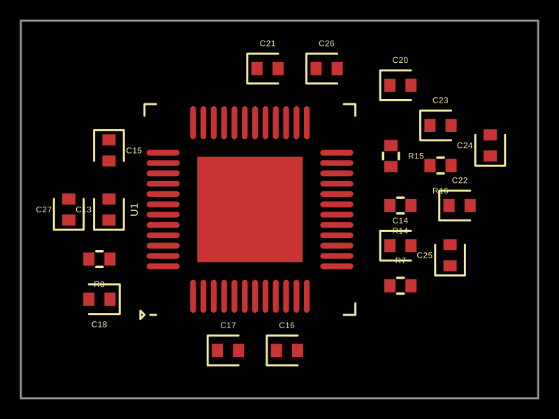 Similar packageMustafaMulla29/ti-chipThis code models a hardware circuit for a motor driver using a DRV83053QPHPQ1 integrated circuit, with power supply bypass capacitors, charge-pump capacitors, resistors, and filters, representing the physical connections and key components in a motor control power stage.
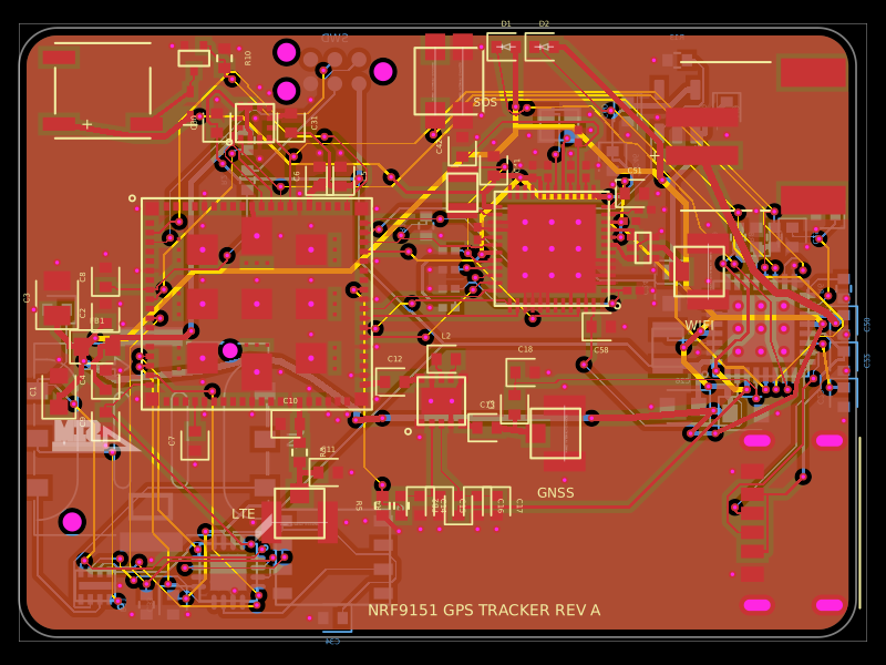 Discover something newpixalynx/nrf9151-gps-trackerA compact 44×32 mm, 4-layer nRF9151 LTE-M/NB-IoT/GNSS tracker PCB with nPM1300 LiPo/USB-C power, nano-SIM/eSIM switching, nRF7002 Wi‑Fi scanning, accelerometer, antennas, buzzer, LEDs, SOS button, and SWD/debug connectors.