imrishabh18/aux
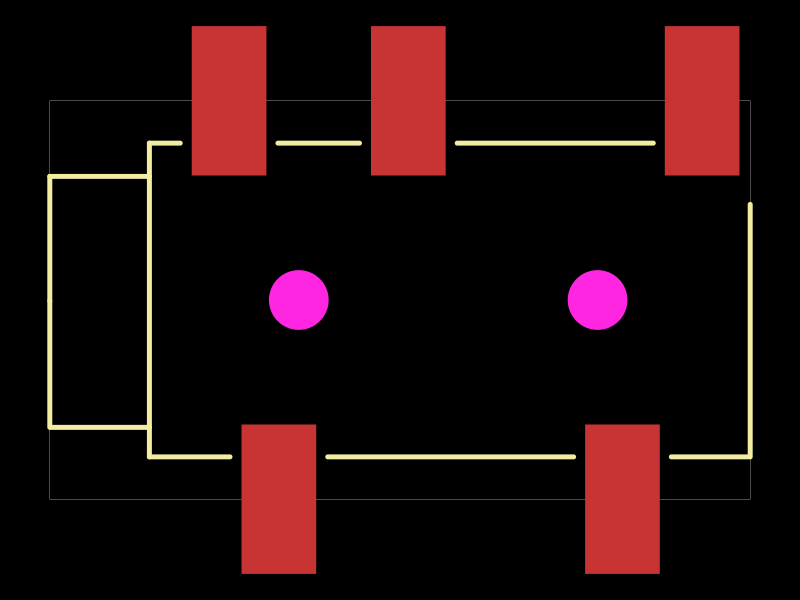
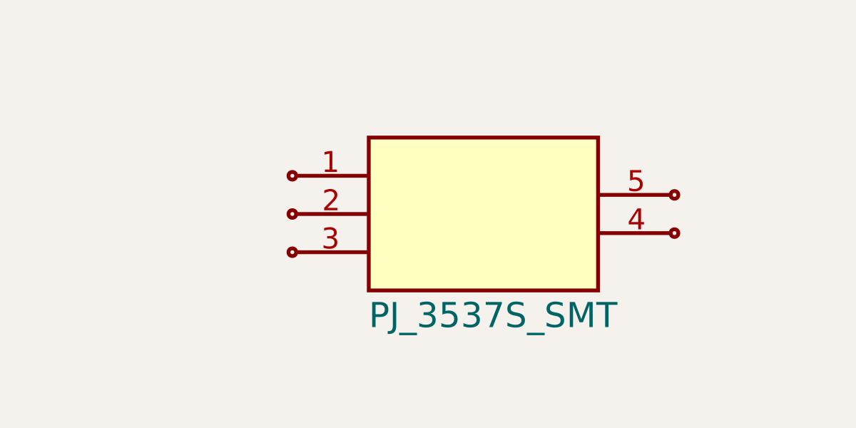
This code defines an SMT surface-mount electronic component with five pins, including its physical footprint and 3D model for PCB integration.
Usage: To import and use the PJ_3537S_SMT component: 1. Import the component: ```tsx import { PJ_3537S_SMT } from "@tsci/imrishabh18.aux" ``` 2. Use in a circuit: ```tsx <board> <PJ_3537S_SMT name="J1" /> </board> ``` The component has 5 pins (pin1 through pin5) and can be positioned and connected using standard tscircuit tracing methods.
- Version
- 0.0.1
- License
- unset
- Stars
- 0
dist/pcb.svg
PCB
Schematic
<svg xmlns="http://www.w3.org/2000/svg" width="800" height="600" data-software-used-string="@tscircuit/core@0.0.747"><style></style><rect class="boundary" x="0" y="0" fill="#000" width="800" height="600" data-type="pcb_background" data-pcb-layer="global"/><rect class="pcb-boundary" fill="none" stroke="#fff" stroke-width="0.3" x="49.797709255576706" y="100.80956135936913" width="700.4045814888467" height="398.38087728126175" data-type="pcb_boundary" data-pcb-layer="global"/><rect class="pcb-pad" fill="rgb(200, 52, 52)" x="241.51850644718004" y="424.4940241503936" width="74.69641449023726" height="149.39282898047452" data-type="pcb_smtpad" data-pcb-layer="top"/><rect class="pcb-pad" fill="rgb(200, 52, 52)" x="191.7208967870273" y="26.113146869131867" width="74.69641449023726" height="149.39282898047452" data-type="pcb_smtpad" data-pcb-layer="top"/><rect class="pcb-pad" fill="rgb(200, 52, 52)" x="370.98976183995796" y="26.113146869131867" width="74.69641449023726" height="149.39282898047452" data-type="pcb_smtpad" data-pcb-layer="top"/><rect class="pcb-pad" fill="rgb(200, 52, 52)" x="585.1182185168251" y="424.4940241503936" width="74.69641449023726" height="149.39282898047452" data-type="pcb_smtpad" data-pcb-layer="top"/><rect class="pcb-pad" fill="rgb(200, 52, 52)" x="664.8045128676032" y="26.113146869131867" width="74.69641449023726" height="149.39282898047452" data-type="pcb_smtpad" data-pcb-layer="top"/><path class="pcb-silkscreen pcb-silkscreen-top" d="M 457.19958100207526 143.1368971396001 L 653.2885784721016 143.1368971396001" fill="none" stroke="#f2eda1" stroke-width="4.979770925557669" stroke-linecap="round" stroke-linejoin="round" data-pcb-component-id="pcb_component_0" data-pcb-silkscreen-path-id="pcb_silkscreen_path_0" data-type="pcb_silkscreen_path" data-pcb-layer="top"/><path class="pcb-silkscreen pcb-silkscreen-top" d="M 277.92818622550607 143.1368971396001 L 359.4814166153493 143.1368971396001" fill="none" stroke="#f2eda1" stroke-width="4.979770925557669" stroke-linecap="round" stroke-linejoin="round" data-pcb-component-id="pcb_component_0" data-pcb-silkscreen-path-id="pcb_silkscreen_path_1" data-type="pcb_silkscreen_path" data-pcb-layer="top"/><path class="pcb-silkscreen pcb-silkscreen-top" d="M 149.39292857588794 143.1368971396001 L 180.21002183879142 143.1368971396001" fill="none" stroke="#f2eda1" stroke-width="4.979770925557669" stroke-linecap="round" stroke-linejoin="round" data-pcb-component-id="pcb_component_0" data-pcb-silkscreen-path-id="pcb_silkscreen_path_2" data-type="pcb_silkscreen_path" data-pcb-layer="top"/><path class="pcb-silkscreen pcb-silkscreen-top" d="M 671.3305674025752 456.86310286040555 L 750.2022907444234 456.86310286040555 L 750.2022907444234 204.40047915355632" fill="none" stroke="#f2eda1" stroke-width="4.979770925557669" stroke-linecap="round" stroke-linejoin="round" data-pcb-component-id="pcb_component_0" data-pcb-silkscreen-path-id="pcb_silkscreen_path_3" data-type="pcb_silkscreen_path" data-pcb-layer="top"/><path class="pcb-silkscreen pcb-silkscreen-top" d="M 327.72579588565884 456.86310286040555 L 573.6124030158436 456.86310286040555" fill="none" stroke="#f2eda1" stroke-width="4.979770925557669" stroke-linecap="round" stroke-linejoin="round" data-pcb-component-id="pcb_component_0" data-pcb-silkscreen-path-id="pcb_silkscreen_path_4" data-type="pcb_silkscreen_path" data-pcb-layer="top"/><path class="pcb-silkscreen pcb-silkscreen-top" d="M 149.39292857588794 456.86310286040555 L 230.008896360755 456.86310286040555" fill="none" stroke="#f2eda1" stroke-width="4.979770925557669" stroke-linecap="round" stroke-linejoin="round" data-pcb-component-id="pcb_component_0" data-pcb-silkscreen-path-id="pcb_silkscreen_path_5" data-type="pcb_silkscreen_path" data-pcb-layer="top"/><path class="pcb-silkscreen pcb-silkscreen-top" d="M 49.797709255576706 300.8904627178278 L 49.797709255576706 427.37664422698515 L 149.39292857588794 427.37664422698515" fill="none" stroke="#f2eda1" stroke-width="4.979770925557669" stroke-linecap="round" stroke-linejoin="round" data-pcb-component-id="pcb_component_0" data-pcb-silkscreen-path-id="pcb_silkscreen_path_6" data-type="pcb_silkscreen_path" data-pcb-layer="top"/><path class="pcb-silkscreen pcb-silkscreen-top" d="M 49.797709255576706 176.39643856743174 L 149.39292857588794 176.39643856743174" fill="none" stroke="#f2eda1" stroke-width="4.979770925557669" stroke-linecap="round" stroke-linejoin="round" data-pcb-component-id="pcb_component_0" data-pcb-silkscreen-path-id="pcb_silkscreen_path_7" data-type="pcb_silkscreen_path" data-pcb-layer="top"/><path class="pcb-silkscreen pcb-silkscreen-top" d="M 49.797709255576706 300.8904627178278 L 49.797709255576706 176.39643856743174" fill="none" stroke="#f2eda1" stroke-width="4.979770925557669" stroke-linecap="round" stroke-linejoin="round" data-pcb-component-id="pcb_component_0" data-pcb-silkscreen-path-id="pcb_silkscreen_path_8" data-type="pcb_silkscreen_path" data-pcb-layer="top"/><path class="pcb-silkscreen pcb-silkscreen-top" d="M 149.39292857588794 143.1368971396001 L 149.39292857588794 456.86310286040555" fill="none" stroke="#f2eda1" stroke-width="4.979770925557669" stroke-linecap="round" stroke-linejoin="round" data-pcb-component-id="pcb_component_0" data-pcb-silkscreen-path-id="pcb_silkscreen_path_9" data-type="pcb_silkscreen_path" data-pcb-layer="top"/><circle class="pcb-hole" cx="298.7857575563688" cy="300.00505944726285" r="29.8785657960949" fill="#FF26E2" data-type="pcb_hole" data-pcb-layer="drill"/><circle class="pcb-hole" cx="597.5739452409466" cy="300.00505944726285" r="29.8785657960949" fill="#FF26E2" data-type="pcb_hole" data-pcb-layer="drill"/></svg>