hrithik18k/Chatting-Device
This code defines React components representing surface-mount voltage regulator and resistor chips with specified pin layouts, footprints, and 3D CAD models for electronic hardware design.
- Version
- 1.0.0
- License
- unset
- Stars
- 0
imports/HS28QI084RX.tsx
import type { ChipProps } from "@tscircuit/props"

const pinLabels = {
  pin1: ["DB0"],
  pin2: ["DB1"],
  pin3: ["DB2"],
  pin4: ["DB3"],
  pin5: ["GND1"],
  pin6: ["IOVCC1"],
  pin7: ["CS"],
  pin8: ["RS"],
  pin9: ["WR"],
  pin10: ["RD"],
  pin11: ["IM0"],
  pin12: ["X_POS"],
  pin13: ["Y_POS"],
  pin14: ["X_NEG"],
  pin15: ["Y_NEG"],
  pin16: ["LEDA"],
  pin17: ["LEDK1"],
  pin18: ["LEDK2"],
  pin19: ["LEDK3"],
  pin20: ["LEDK4"],
  pin21: ["NC"],
  pin22: ["DB4"],
  pin23: ["DB8"],
  pin24: ["DB9"],
  pin25: ["DB10"],
  pin26: ["DB11"],
  pin27: ["DB12"],
  pin28: ["DB13"],
  pin29: ["DB14"],
  pin30: ["DB15"],
  pin31: ["RESET"],
  pin32: ["VCC"],
  pin33: ["IOVCC2"],
  pin34: ["GND2"],
  pin35: ["DB5"],
  pin36: ["DB6"],
  pin37: ["DB7"]
} as const

export const HS28QI084RX = (props: ChipProps<typeof pinLabels>) => {
  return (
    <chip
      pinLabels={pinLabels}
      symbol={
        <symbol>
          <schematicrect schX={0} schY={1.27} width={96.52} height={81.28} strokeWidth={0.254} color="#880000" />
          <schematiccircle center={{ x: -46.99, y: -38.1 }} radius={0.381} strokeWidth={0.254} color="#880000" isFilled fillColor="#880000" />
          <port name="pin1" pinNumber={1} aliases={["DB0"]} direction="down" schX={-45.72} schY={-41.91} schStemLength={2.54} />
          <port name="pin2" pinNumber={2} aliases={["DB1"]} direction="down" schX={-43.18} schY={-41.91} schStemLength={2.54} />
          <port name="pin3" pinNumber={3} aliases={["DB2"]} direction="down" schX={-40.64} schY={-41.91} schStemLength={2.54} />
          <port name="pin4" pinNumber={4} aliases={["DB3"]} direction="down" schX={-38.1} schY={-41.91} schStemLength={2.54} />
          <port name="pin5" pinNumber={5} aliases={["GND1","GND"]} direction="down" schX={-35.56} schY={-41.91} schStemLength={2.54} />
          <port name="pin6" pinNumber={6} aliases={["IOVCC1","IOVCC"]} direction="down" schX={-33.02} schY={-41.91} schStemLength={2.54} />
          <port name="pin7" pinNumber={7} aliases={["CS"]} direction="down" schX={-30.48} schY={-41.91} schStemLength={2.54} />
          <port name="pin8" pinNumber={8} aliases={["RS"]} direction="down" schX={-27.94} schY={-41.91} schStemLength={2.54} />
          <port name="pin9" pinNumber={9} aliases={["WR"]} direction="down" schX={-25.4} schY={-41.91} schStemLength={2.54} />
          <port name="pin10" pinNumber={10} aliases={["RD"]} direction="down" schX={-22.86} schY={-41.91} schStemLength={2.54} />
          <port name="pin11" pinNumber={11} aliases={["IM0"]} direction="down" schX={-20.32} schY={-41.91} schStemLength={2.54} />
          <port name="pin12" pinNumber={12} aliases={["X_POS"]} direction="down" schX={-17.78} schY={-41.91} schStemLength={2.54} />
          <port name="pin13" pinNumber={13} aliases={["Y_POS"]} direction="down" schX={-15.24} schY={-41.91} schStemLength={2.54} />
          <port name="pin14" pinNumber={14} aliases={["X_NEG"]} direction="down" schX={-12.7} schY={-41.91} schStemLength={2.54} />
          <port name="pin15" pinNumber={15} aliases={["Y_NEG"]} direction="down" schX={-10.16} schY={-41.91} schStemLength={2.54} />
          <port name="pin16" pinNumber={16} aliases={["LEDA"]} direction="down" schX={-7.62} schY={-41.91} schStemLength={2.54} />
          <port name="pin17" pinNumber={17} aliases={["LEDK1"]} direction="down" schX={-5.08} schY={-41.91} schStemLength={2.54} />
          <port name="pin18" pinNumber={18} aliases={["LEDK2"]} direction="down" schX={-2.54} schY={-41.91} schStemLength={2.54} />
          <port name="pin19" pinNumber={19} aliases={["LEDK3"]} direction="down" schX={0} schY={-41.91} schStemLength={2.54} />
          <port name="pin20" pinNumber={20} aliases={["LEDK4"]} direction="down" schX={2.54} schY={-41.91} schStemLength={2.54} />
          <port name="pin21" pinNumber={21} aliases={["NC"]} direction="down" schX={5.08} schY={-41.91} schStemLength={2.54} />
          <port name="pin22" pinNumber={22} aliases={["DB4"]} direction="down" schX={7.62} schY={-41.91} schStemLength={2.54} />
          <port name="pin23" pinNumber={23} aliases={["DB8"]} direction="down" schX={10.16} schY={-41.91} schStemLength={2.54} />
          <port name="pin24" pinNumber={24} aliases={["DB9"]} direction="down" schX={12.7} schY={-41.91} schStemLength={2.54} />
          <port name="pin25" pinNumber={25} aliases={["DB10"]} direction="down" schX={15.24} schY={-41.91} schStemLength={2.54} />
          <port name="pin26" pinNumber={26} aliases={["DB11"]} direction="down" schX={17.78} schY={-41.91} schStemLength={2.54} />
          <port name="pin27" pinNumber={27} aliases={["DB12"]} direction="down" schX={20.32} schY={-41.91} schStemLength={2.54} />
          <port name="pin28" pinNumber={28} aliases={["DB13"]} direction="down" schX={22.86} schY={-41.91} schStemLength={2.54} />
          <port name="pin29" pinNumber={29} aliases={["DB14"]} direction="down" schX={25.4} schY={-41.91} schStemLength={2.54} />
          <port name="pin30" pinNumber={30} aliases={["DB15"]} direction="down" schX={27.94} schY={-41.91} schStemLength={2.54} />
          <port name="pin31" pinNumber={31} aliases={["RESET"]} direction="down" schX={30.48} schY={-41.91} schStemLength={2.54} />
          <port name="pin32" pinNumber={32} aliases={["VCC"]} direction="down" schX={33.02} schY={-41.91} schStemLength={2.54} />
          <port name="pin33" pinNumber={33} aliases={["IOVCC2","IOVCC"]} direction="down" schX={35.56} schY={-41.91} schStemLength={2.54} />
          <port name="pin34" pinNumber={34} aliases={["GND2","GND"]} direction="down" schX={38.1} schY={-41.91} schStemLength={2.54} />
          <port name="pin35" pinNumber={35} aliases={["DB5"]} direction="down" schX={40.64} schY={-41.91} schStemLength={2.54} />
          <port name="pin36" pinNumber={36} aliases={["DB6"]} direction="down" schX={43.18} schY={-41.91} schStemLength={2.54} />
          <port name="pin37" pinNumber={37} aliases={["DB7"]} direction="down" schX={45.72} schY={-41.91} schStemLength={2.54} />
          <schematicrect schX={0} schY={5.715} width={88.9} height={67.31} strokeWidth={0.254} color="#000000" />
          <schematictext schX={-2.54} schY={-1.27} text="LCD" fontSize={3.175} anchor="left" color="#0000FF" schRotation={0} />
        </symbol>
      }
      supplierPartNumbers={{
  "jlcpcb": [
    "C18198245"
  ]
}}
      manufacturerPartNumber="HS28QI084RX"
      footprint={<footprint>
        <smtpad portHints={["pin1"]} pcbX="0mm" pcbY="17.999964mm" width="3.999992mm" height="0.6999986mm" shape="rect" />
<smtpad portHints={["pin2"]} pcbX="0mm" pcbY="16.999966mm" width="3.999992mm" height="0.6999986mm" shape="rect" />
<smtpad portHints={["pin3"]} pcbX="0mm" pcbY="15.999968mm" width="3.999992mm" height="0.6999986mm" shape="rect" />
<smtpad portHints={["pin4"]} pcbX="0mm" pcbY="14.99997mm" width="3.999992mm" height="0.6999986mm" shape="rect" />
<smtpad portHints={["pin5"]} pcbX="0mm" pcbY="13.999972mm" width="3.999992mm" height="0.6999986mm" shape="rect" />
<smtpad portHints={["pin6"]} pcbX="0mm" pcbY="12.999974mm" width="3.999992mm" height="0.6999986mm" shape="rect" />
<smtpad portHints={["pin7"]} pcbX="0mm" pcbY="11.999976mm" width="3.999992mm" height="0.6999986mm" shape="rect" />
<smtpad portHints={["pin8"]} pcbX="0mm" pcbY="10.999978mm" width="3.999992mm" height="0.6999986mm" shape="rect" />
<smtpad portHints={["pin9"]} pcbX="0mm" pcbY="9.99998mm" width="3.999992mm" height="0.6999986mm" shape="rect" />
<smtpad portHints={["pin10"]} pcbX="0mm" pcbY="8.999982mm" width="3.999992mm" height="0.6999986mm" shape="rect" />
<smtpad portHints={["pin11"]} pcbX="0mm" pcbY="7.999984mm" width="3.999992mm" height="0.6999986mm" shape="rect" />
<smtpad portHints={["pin12"]} pcbX="0mm" pcbY="6.999986mm" width="3.999992mm" height="0.6999986mm" shape="rect" />
<smtpad portHints={["pin13"]} pcbX="0mm" pcbY="5.999988mm" width="3.999992mm" height="0.6999986mm" shape="rect" />
<smtpad portHints={["pin14"]} pcbX="0mm" pcbY="4.99999mm" width="3.999992mm" height="0.6999986mm" shape="rect" />
<smtpad portHints={["pin15"]} pcbX="0mm" pcbY="3.999992mm" width="3.999992mm" height="0.6999986mm" shape="rect" />
<smtpad portHints={["pin16"]} pcbX="0mm" pcbY="2.999994mm" width="3.999992mm" height="0.6999986mm" shape="rect" />
<smtpad portHints={["pin17"]} pcbX="0mm" pcbY="1.999996mm" width="3.999992mm" height="0.6999986mm" shape="rect" />
<smtpad portHints={["pin18"]} pcbX="0mm" pcbY="0.999998mm" width="3.999992mm" height="0.6999986mm" shape="rect" />
<smtpad portHints={["pin19"]} pcbX="0mm" pcbY="0mm" width="3.999992mm" height="0.6999986mm" shape="rect" />
<smtpad portHints={["pin20"]} pcbX="0mm" pcbY="-0.999998mm" width="3.999992mm" height="0.6999986mm" shape="rect" />
<smtpad portHints={["pin21"]} pcbX="0mm" pcbY="-1.999996mm" width="3.999992mm" height="0.6999986mm" shape="rect" />
<smtpad portHints={["pin22"]} pcbX="0mm" pcbY="-2.999994mm" width="3.999992mm" height="0.6999986mm" shape="rect" />
<smtpad portHints={["pin23"]} pcbX="0mm" pcbY="-3.999992mm" width="3.999992mm" height="0.6999986mm" shape="rect" />
<smtpad portHints={["pin24"]} pcbX="0mm" pcbY="-4.99999mm" width="3.999992mm" height="0.6999986mm" shape="rect" />
<smtpad portHints={["pin25"]} pcbX="0mm" pcbY="-5.999988mm" width="3.999992mm" height="0.6999986mm" shape="rect" />
<smtpad portHints={["pin26"]} pcbX="0mm" pcbY="-6.999986mm" width="3.999992mm" height="0.6999986mm" shape="rect" />
<smtpad portHints={["pin27"]} pcbX="0mm" pcbY="-7.999984mm" width="3.999992mm" height="0.6999986mm" shape="rect" />
<smtpad portHints={["pin28"]} pcbX="0mm" pcbY="-8.999982mm" width="3.999992mm" height="0.6999986mm" shape="rect" />
<smtpad portHints={["pin29"]} pcbX="0mm" pcbY="-9.99998mm" width="3.999992mm" height="0.6999986mm" shape="rect" />
<smtpad portHints={["pin30"]} pcbX="0mm" pcbY="-10.999978mm" width="3.999992mm" height="0.6999986mm" shape="rect" />
<smtpad portHints={["pin31"]} pcbX="0mm" pcbY="-11.999976mm" width="3.999992mm" height="0.6999986mm" shape="rect" />
<smtpad portHints={["pin32"]} pcbX="0mm" pcbY="-12.999974mm" width="3.999992mm" height="0.6999986mm" shape="rect" />
<smtpad portHints={["pin33"]} pcbX="0mm" pcbY="-13.999972mm" width="3.999992mm" height="0.6999986mm" shape="rect" />
<smtpad portHints={["pin34"]} pcbX="0mm" pcbY="-14.99997mm" width="3.999992mm" height="0.6999986mm" shape="rect" />
<smtpad portHints={["pin35"]} pcbX="0mm" pcbY="-15.999968mm" width="3.999992mm" height="0.6999986mm" shape="rect" />
<smtpad portHints={["pin36"]} pcbX="0mm" pcbY="-16.999966mm" width="3.999992mm" height="0.6999986mm" shape="rect" />
<smtpad portHints={["pin37"]} pcbX="0mm" pcbY="-17.999964mm" width="3.999992mm" height="0.6999986mm" shape="rect" />
<silkscreenpath route={[{"x":0.7618984000000637,"y":18.66902540000001},{"x":0.7618984000000637,"y":21.08197460000008},{"x":-28.200045199999863,"y":21.08197460000008}]} />
<silkscreenpath route={[{"x":0.7618984000000637,"y":-18.79597459999991},{"x":0.7618984000000637,"y":-21.081847599999946},{"x":-28.200045199999863,"y":-21.081847599999946}]} />
<silkscreenpath route={[{"x":41.29976499999998,"y":25.000000799999953},{"x":41.29976499999998,"y":-24.999873799999932}]} />
<silkscreenpath route={[{"x":-28.200045199999863,"y":25.000000799999953},{"x":41.29976499999998,"y":25.000000799999953}]} />
<silkscreenpath route={[{"x":-28.200045199999863,"y":-24.999873799999932},{"x":41.29976499999998,"y":-24.999873799999932}]} />
<silkscreenpath route={[{"x":-28.200045199999863,"y":-24.999873799999932},{"x":-28.200045199999863,"y":25.000000799999953}]} />
<silkscreentext text="{NAME}" pcbX="6.399276mm" pcbY="26.149302mm" anchorAlignment="center" fontSize="1mm" />
<courtyardoutline outline={[{"x":-28.851923999999826,"y":25.399302000000034},{"x":41.65047600000025,"y":25.399302000000034},{"x":41.65047600000025,"y":-25.392697999999882},{"x":-28.851923999999826,"y":-25.392697999999882},{"x":-28.851923999999826,"y":25.399302000000034}]} />
      </footprint>}
      cadModel={{
        objUrl: "https://modelcdn.tscircuit.com/easyeda_models/assets/C18198245.obj?uuid=beb9d7b2ed4b40f6814fc5ad10193210",
        stepUrl: "https://modelcdn.tscircuit.com/easyeda_models/assets/C18198245.step?uuid=beb9d7b2ed4b40f6814fc5ad10193210",
        pcbRotationOffset: 270,
        modelOriginPosition: { x: 0.00005080000005364127, y: -6.699886200000183, z: -3.81 },
      }}
      {...props}
    />
  )
}
Related Packages
 More from this authorhrithik18k/smart-switch-pcbThe AO3400A component models a SOT-23 N-channel MOSFET with labeled pins for Gate, Source, and Drain, including 3D CAD models and schematic symbols for electronic circuit design.
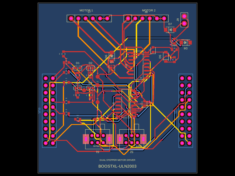 Similar packageabse/boostxl-uln2003This code defines a React component that models a through-hole or surface-mount LED with specified pin labels, footprint, silkscreen, and 3D CAD model for PCB layout.
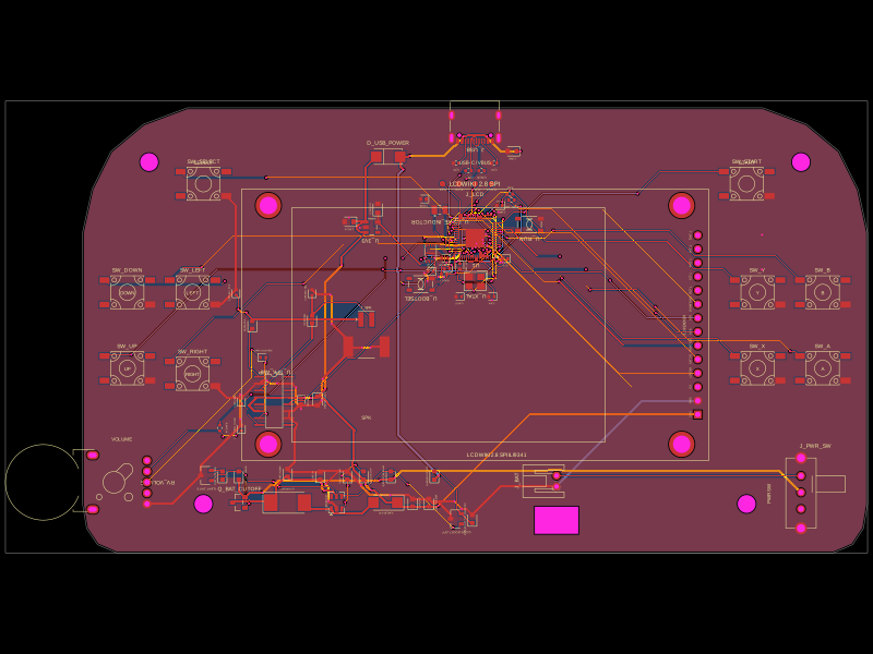 Discover something newabse/gameboy-advanceThis code defines a collection of hardware components, including microcontrollers, sensors, display modules, power management ICs, and passive/passive components, each modeled as 3D symbols with specific footprints, pin configurations, and associated models for PCB and schematic design.