gokul/new-clock
This code defines a PCB schematic with physical hardware components including switches, chips, resistors, capacitors, inductors, connectors, and visual annotations for a six-digit 12-hour digital clock circuit.
- Version
- 0.0.1
- License
- unset
- Stars
- 0
index.tsx
PCB
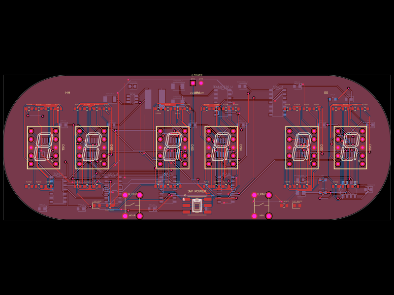
Schematic

import { FJ3191AH } from "./imports/c44296"
import { YTSPS_22E58LM } from "./imports/c2941005"

const cd4026Pins = {
  pin1: ["CLOCK"], pin2: ["CLOCK_INHIBIT"],
  pin3: ["DISPLAY_ENABLE_IN"], pin4: ["DISPLAY_ENABLE_OUT"],
  pin5: ["CARRY_OUT"], pin6: ["F"], pin7: ["G"], pin8: ["VSS"],
  pin9: ["D"], pin10: ["A"], pin11: ["E"], pin12: ["B"],
  pin13: ["C"], pin14: ["UNGATED_C"], pin15: ["RESET"], pin16: ["VDD"],
} as const

const quadGatePins = {
  pin1: ["A1"], pin2: ["B1"], pin3: ["Y1"],
  pin4: ["A2"], pin5: ["B2"], pin6: ["Y2"], pin7: ["VSS"],
  pin8: ["Y3"], pin9: ["A3"], pin10: ["B3"],
  pin11: ["Y4"], pin12: ["A4"], pin13: ["B4"], pin14: ["VDD"],
} as const

const cd4093Pins = {
  pin1: ["A1"], pin2: ["B1"], pin3: ["Y1"],
  pin4: ["Y2"], pin5: ["B2"], pin6: ["A2"], pin7: ["VSS"],
  pin8: ["A3"], pin9: ["B3"], pin10: ["Y3"],
  pin11: ["Y4"], pin12: ["B4"], pin13: ["A4"], pin14: ["VDD"],
} as const

const cd4069Pins = {
  pin1: ["A1"], pin2: ["Y1"], pin3: ["A2"], pin4: ["Y2"],
  pin5: ["A3"], pin6: ["Y3"], pin7: ["VSS"], pin8: ["Y4"],
  pin9: ["A4"], pin10: ["Y5"], pin11: ["A5"], pin12: ["Y6"],
  pin13: ["A6"], pin14: ["VDD"],
} as const

const timerPins = {
  pin1: ["GND"], pin2: ["TRIGGER"], pin3: ["OUTPUT"], pin4: ["RESET"],
  pin5: ["CONTROL"], pin6: ["THRESHOLD"], pin7: ["DISCHARGE"], pin8: ["VDD"],
} as const

const segments = ["A", "B", "C", "D", "E", "F", "G"] as const

const digits = [
  { display: "DS1", role: "H10", x: -47.5, clock: "H10_CLOCK", reset: "HOUR_RESET" },
  { display: "DS2", role: "H1",  x: -32.5, clock: "H1_CLOCK",  reset: "HOUR_RESET" },
  { display: "DS3", role: "M10", x: -7.5,  clock: "M10_CLOCK", reset: "MIN10_RESET" },
  { display: "DS4", role: "M1",  x: 7.5,   clock: "M1_CLOCK",  reset: "POR" },
  { display: "DS5", role: "S10", x: 32.5,  clock: "S10_CLOCK", reset: "SEC10_RESET" },
  { display: "DS6", role: "S1",  x: 47.5,  clock: "CLOCK_1HZ", reset: "POR" },
] as const

function DigitBlock({ display, role, x, clock, reset }: (typeof digits)[number]) {
  const resistorX = [x - 4.5, x - 1.5, x + 1.5, x + 4.5]
  return (
    <>
      <FJ3191AH
        name={display}
        pcbX={x}
        pcbY={0}
        pcbRotation="270deg"
        noConnect={["dp"]}
        connections={{
          GND1: "net.GND",
          GND2: "net.GND",
          a: `net.${role}_A_LED`, b: `net.${role}_B_LED`,
          c: `net.${role}_C_LED`, d: `net.${role}_D_LED`,
          e: `net.${role}_E_LED`, f: `net.${role}_F_LED`,
          g: `net.${role}_G_LED`,
        }}
      />

      {segments.map((segment, index) => (
        <resistor
          key={`${display}-${segment}`}
          name={`R_${display}_${segment}`}
          resistance="220ohm"
          footprint="0603"
          pcbX={resistorX[index % 4]}
          pcbY={index < 4 ? 12 : -12}
          connections={{
            pin1: `net.${role}_${segment}_RAW`,
            pin2: `net.${role}_${segment}_LED`,
          }}
        />
      ))}

      <chip
        name={`U_${display}`}
        manufacturerPartNumber="CD4026BPWR"
        footprint="tssop16"
        pinLabels={cd4026Pins}
        pinAttributes={{
          pin8: { requiresGround: true },
          pin16: { requiresPower: true },
        }}
        pcbX={x}
        pcbY={0}
        pcbRotation="90deg"
        layer="bottom"
        noConnect={["DISPLAY_ENABLE_OUT", "UNGATED_C"]}
        connections={{
          VDD: "net.V5",
          VSS: "net.GND",
          CLOCK: `net.${clock}`,
          CLOCK_INHIBIT: "net.GND",
          DISPLAY_ENABLE_IN: "net.V5",
          CARRY_OUT: `net.${role}_CARRY`,
          RESET: `net.${reset}`,
          A: `net.${role}_A_RAW`, B: `net.${role}_B_RAW`,
          C: `net.${role}_C_RAW`, D: `net.${role}_D_RAW`,
          E: `net.${role}_E_RAW`, F: `net.${role}_F_RAW`,
          G: `net.${role}_G_RAW`,
        }}
      />

      <capacitor
        name={`C_U_${display}`}
        capacitance="100nF"
        footprint="0603"
        pcbX={x + 6}
        pcbY={7}
        layer="bottom"
        connections={{ pin1: "net.V5", pin2: "net.GND" }}
      />
    </>
  )
}

export default function ClockBoard() {
  return (
    <board
      width="120mm"
      height="45mm"
      borderRadius="20mm"
      layers={2}
      thickness="1.6mm"
      title="Six Digit 12 Hour Logic Clock"
      minViaHoleDiameter="0.3mm"
      minViaPadDiameter="0.55mm"
      autorouter={{
        serverUrl: "https://api.tscircuit.com",
        serverMode: "job",
        inputFormat: "simplified",
      }}
    >
      {/* Call the renderer as a plain function so tscircuit keeps every pcbX/pcbY absolute. */}
      {digits.map((digit) => DigitBlock(digit))}

      {/* 2S protected-battery input and power switch. */}
      <pinheader
        name="J_POWER"
        pinCount={2}
        pitch="2.54mm"
        footprint="pinrow2_p2.54"
        pcbX={0}
        pcbY={20}
        connections={{ pin1: "net.VBAT_2S", pin2: "net.GND" }}
      />
      <YTSPS_22E58LM
        name="SW_POWER"
        pcbX={0}
        pcbY={-18}
        layer="top"
        connections={{
          pin2: "net.VBAT_2S", pin5: "net.VBAT_2S",
          pin1: "net.VBAT_SW", pin4: "net.VBAT_SW",
          pin3: "net.SWITCH_NC_3", pin6: "net.SWITCH_NC_6",
        }}
      />

      {/* AP63205 fixed 5 V buck stage for a 2S Li-ion battery. */}
      <chip
        name="U_BUCK"
        manufacturerPartNumber="AP63205WU-7"
        footprint="sot23_6"
        pinLabels={{
          pin1: ["FB"], pin2: ["EN"], pin3: ["VIN"],
          pin4: ["GND"], pin5: ["SW"], pin6: ["BST"],
        }}
        pinAttributes={{
          pin3: { requiresPower: true },
          pin4: { requiresGround: true },
        }}
        pcbX={-20}
        pcbY={15}
        layer="bottom"
        connections={{
          FB: "net.V5", EN: "net.VBAT_SW", VIN: "net.VBAT_SW",
          GND: "net.GND", SW: "net.BUCK_SW", BST: "net.BUCK_BST",
        }}
      />
      <capacitor name="C_BUCK_IN" capacitance="10uF" footprint="1206"
        pcbX={-27} pcbY={15} layer="bottom"
        connections={{ pin1: "net.VBAT_SW", pin2: "net.GND" }} />
      <capacitor name="C_BUCK_BOOT" capacitance="100nF" footprint="0603"
        pcbX={-20} pcbY={19} layer="bottom"
        connections={{ pin1: "net.BUCK_BST", pin2: "net.BUCK_SW" }} />
      <inductor
        name="L_BUCK"
        manufacturerPartNumber="SRN6045-4R7Y"
        inductance="4.7uH"
        pcbX={-13}
        pcbY={15}
        layer="bottom"
        footprint={
          <footprint>
            <smtpad portHints={["pin1"]} pcbX={-2.15} pcbY={0}
              width="2mm" height="6mm" shape="rect" />
            <smtpad portHints={["pin2"]} pcbX={2.15} pcbY={0}
              width="2mm" height="6mm" shape="rect" />
            <courtyardoutline outline={[
              { x: -3.5, y: -3.5 }, { x: 3.5, y: -3.5 },
              { x: 3.5, y: 3.5 }, { x: -3.5, y: 3.5 },
              { x: -3.5, y: -3.5 },
            ]} />
          </footprint>
        }
        connections={{ pin1: "net.BUCK_SW", pin2: "net.V5" }}
      />
      <capacitor name="C_BUCK_OUT1" capacitance="22uF" footprint="1206"
        pcbX={-6} pcbY={14} layer="bottom"
        connections={{ pin1: "net.V5", pin2: "net.GND" }} />
      <capacitor name="C_BUCK_OUT2" capacitance="22uF" footprint="1206"
        pcbX={-6} pcbY={19} layer="bottom"
        connections={{ pin1: "net.V5", pin2: "net.GND" }} />

      {/* TLC555 astable source; nominally close to 1 Hz. */}
      <chip
        name="U_TIMER"
        manufacturerPartNumber="TLC555IDR"
        footprint="soic8"
        pinLabels={timerPins}
        pinAttributes={{
          pin1: { requiresGround: true },
          pin8: { requiresPower: true },
        }}
        pcbX={47}
        pcbY={-13}
        pcbRotation="90deg"
        layer="bottom"
        connections={{
          VDD: "net.V5", GND: "net.GND", RESET: "net.V5",
          OUTPUT: "net.CLOCK_1HZ", TRIGGER: "net.TIMER_RC",
          THRESHOLD: "net.TIMER_RC", DISCHARGE: "net.TIMER_DISCHARGE",
          CONTROL: "net.TIMER_CONTROL",
        }}
      />
      <resistor name="R_TIMER_A" resistance="4.7kohm" footprint="0603"
        pcbX={39} pcbY={-10} layer="bottom"
        connections={{ pin1: "net.V5", pin2: "net.TIMER_DISCHARGE" }} />
      <resistor name="R_TIMER_B" resistance="68kohm" footprint="0603"
        pcbX={39} pcbY={-14} layer="bottom"
        connections={{ pin1: "net.TIMER_DISCHARGE", pin2: "net.TIMER_RC" }} />
      <capacitor name="C_TIMER" capacitance="10uF" footprint="0805"
        pcbX={32} pcbY={-14} layer="bottom"
        connections={{ pin1: "net.TIMER_RC", pin2: "net.GND" }} />
      <capacitor name="C_TIMER_CONTROL" capacitance="10nF" footprint="0603"
        pcbX={32} pcbY={-10} layer="bottom"
        connections={{ pin1: "net.TIMER_CONTROL", pin2: "net.GND" }} />
      <capacitor name="C_TIMER_DECOUPLE" capacitance="100nF" footprint="0603"
        pcbX={53} pcbY={-13} layer="bottom"
        connections={{ pin1: "net.V5", pin2: "net.GND" }} />

      {/* Counter cascade connections. */}
      <trace from="net.S1_CARRY" to="net.S10_CLOCK" />
      <trace from="net.M1_CARRY" to="net.M10_CLOCK" />
      <trace from="net.H1_CARRY" to="net.H10_CLOCK" />

      {/* Detect six on the seconds/minutes tens positions. */}
      <chip
        name="U_NOT"
        manufacturerPartNumber="CD4069UBM96"
        footprint="soic14"
        pinLabels={cd4069Pins}
        pinAttributes={{ pin7: { requiresGround: true }, pin14: { requiresPower: true } }}
        pcbX={-43} pcbY={-13} layer="bottom"
        noConnect={["Y3", "Y4", "Y5", "Y6"]}
        connections={{
          VDD: "net.V5", VSS: "net.GND",
          A1: "net.S10_B_RAW", Y1: "net.S10_NOT_B",
          A2: "net.M10_B_RAW", Y2: "net.M10_NOT_B",
          A3: "net.GND", A4: "net.GND", A5: "net.GND", A6: "net.GND",
        }}
      />
      <chip
        name="U_AND"
        manufacturerPartNumber="CD4081BM96"
        footprint="soic14"
        pinLabels={quadGatePins}
        pinAttributes={{ pin7: { requiresGround: true }, pin14: { requiresPower: true } }}
        pcbX={-26} pcbY={-13} layer="bottom"
        connections={{
          VDD: "net.V5", VSS: "net.GND",
          A1: "net.S10_NOT_B", B1: "net.S10_C_RAW", Y1: "net.S10_DETECT",
          A2: "net.S10_DETECT", B2: "net.S10_E_RAW", Y2: "net.SEC_ROLLOVER",
          A3: "net.M10_NOT_B", B3: "net.M10_C_RAW", Y3: "net.M10_DETECT",
          A4: "net.M10_DETECT", B4: "net.M10_E_RAW", Y4: "net.MIN_ROLLOVER",
        }}
      />

      {/* Detect the transition to 13 and restart the 12-hour cycle at 00. */}
      <chip
        name="U_AND2"
        manufacturerPartNumber="CD4081BM96"
        footprint="soic14"
        pinLabels={quadGatePins}
        pinAttributes={{ pin7: { requiresGround: true }, pin14: { requiresPower: true } }}
        pcbX={-9} pcbY={-13} layer="bottom"
        noConnect={["Y4"]}
        connections={{
          VDD: "net.V5", VSS: "net.GND",
          A1: "net.H1_B_RAW", B1: "net.H1_C_RAW", Y1: "net.HOUR13_1",
          A2: "net.HOUR13_1", B2: "net.H1_G_RAW", Y2: "net.HOUR13_2",
          A3: "net.HOUR13_2", B3: "net.H10_B_RAW", Y3: "net.HOUR_ROLLOVER",
          A4: "net.GND", B4: "net.GND",
        }}
      />

      {/* Hour and minute controls. */}
      <pushbutton
        name="SW_HOUR"
        footprint="pushbutton_id1.3mm_od2mm"
        pcbX={-20} pcbY={-18} layer="top"
        noConnect={["pin3", "pin4"]}
        connections={{ pin1: "net.HOUR_RC", pin2: "net.GND" }}
      />
      <resistor name="R_SET_HOUR" resistance="100kohm" footprint="0603"
        pcbX={-27} pcbY={-18} layer="top"
        connections={{ pin1: "net.V5", pin2: "net.HOUR_RC" }} />
      <capacitor name="C_SET_HOUR" capacitance="100nF" footprint="0603"
        pcbX={-31} pcbY={-18} layer="top"
        connections={{ pin1: "net.HOUR_RC", pin2: "net.GND" }} />

      <pushbutton
        name="SW_MINUTE"
        footprint="pushbutton_id1.3mm_od2mm"
        pcbX={20} pcbY={-18} layer="top"
        noConnect={["pin3", "pin4"]}
        connections={{ pin1: "net.MINUTE_RC", pin2: "net.GND" }}
      />
      <resistor name="R_SET_MINUTE" resistance="100kohm" footprint="0603"
        pcbX={27} pcbY={-18} layer="top"
        connections={{ pin1: "net.V5", pin2: "net.MINUTE_RC" }} />
      <capacitor name="C_SET_MINUTE" capacitance="100nF" footprint="0603"
        pcbX={31} pcbY={-18} layer="top"
        connections={{ pin1: "net.MINUTE_RC", pin2: "net.GND" }} />

      {/* Schmitt debounce and power-on reset. */}
      <resistor name="R_POR" resistance="100kohm" footprint="0603"
        pcbX={42} pcbY={15} layer="bottom"
        connections={{ pin1: "net.V5", pin2: "net.POR_RC" }} />
      <capacitor name="C_POR" capacitance="1uF" footprint="0603"
        pcbX={47} pcbY={15} layer="bottom"
        connections={{ pin1: "net.POR_RC", pin2: "net.GND" }} />
      <chip
        name="U_DEBOUNCE"
        manufacturerPartNumber="CD4093BM96"
        footprint="soic14"
        pinLabels={cd4093Pins}
        pinAttributes={{ pin7: { requiresGround: true }, pin14: { requiresPower: true } }}
        pcbX={8} pcbY={14} layer="bottom"
        noConnect={["Y4"]}
        connections={{
          VDD: "net.V5", VSS: "net.GND",
          A1: "net.HOUR_RC", B1: "net.HOUR_RC", Y1: "net.HOUR_BUTTON",
          A2: "net.MINUTE_RC", B2: "net.MINUTE_RC", Y2: "net.MINUTE_BUTTON",
          A3: "net.POR_RC", B3: "net.POR_RC", Y3: "net.POR",
          A4: "net.GND", B4: "net.GND",
        }}
      />

      {/* OR gates combine rollover pulses, setting buttons and POR. */}
      <chip
        name="U_OR"
        manufacturerPartNumber="CD4071BM96"
        footprint="soic14"
        pinLabels={quadGatePins}
        pinAttributes={{ pin7: { requiresGround: true }, pin14: { requiresPower: true } }}
        pcbX={9} pcbY={-13} layer="bottom"
        connections={{
          VDD: "net.V5", VSS: "net.GND",
          A1: "net.SEC_ROLLOVER", B1: "net.MINUTE_BUTTON", Y1: "net.M1_CLOCK",
          A2: "net.MIN_ROLLOVER", B2: "net.HOUR_BUTTON", Y2: "net.H1_CLOCK",
          A3: "net.POR", B3: "net.SEC_ROLLOVER", Y3: "net.SEC10_RESET",
          A4: "net.POR", B4: "net.MIN_ROLLOVER", Y4: "net.MIN10_RESET",
        }}
      />
      <chip
        name="U_OR2"
        manufacturerPartNumber="CD4071BM96"
        footprint="soic14"
        pinLabels={quadGatePins}
        pinAttributes={{ pin7: { requiresGround: true }, pin14: { requiresPower: true } }}
        pcbX={25} pcbY={14} layer="bottom"
        noConnect={["Y2", "Y3", "Y4"]}
        connections={{
          VDD: "net.V5", VSS: "net.GND",
          A1: "net.POR", B1: "net.HOUR_ROLLOVER", Y1: "net.HOUR_RESET",
          A2: "net.GND", B2: "net.GND",
          A3: "net.GND", B3: "net.GND",
          A4: "net.GND", B4: "net.GND",
        }}
      />

      {[
        { name: "U_NOT", x: -48, y: -19 },
        { name: "U_AND", x: -36, y: -19 },
        { name: "U_AND2", x: -14, y: -19 },
        { name: "U_OR", x: 2, y: -19 },
        { name: "U_DEBOUNCE", x: 14, y: 19 },
        { name: "U_OR2", x: 31, y: 19 },
      ].map(({ name, x, y }) => (
        <capacitor key={name} name={`C_${name}`} capacitance="100nF"
          footprint="0603" pcbX={x} pcbY={y} layer="bottom"
          connections={{ pin1: "net.V5", pin2: "net.GND" }} />
      ))}

      <silkscreentext text="HH" pcbX={-40} pcbY={17} fontSize="1mm" />
      <silkscreentext text="MM" pcbX={0} pcbY={17} fontSize="1mm" />
      <silkscreentext text="SS" pcbX={40} pcbY={17} fontSize="1mm" />
      <silkscreentext text="HOUR" pcbX={-20} pcbY={-21} fontSize="0.7mm" />
      <silkscreentext text="MIN" pcbX={20} pcbY={-21} fontSize="0.7mm" />
      <silkscreentext text="2S BATTERY" pcbX={0} pcbY={17} fontSize="0.7mm" />

      <copperpour connectsTo="net.GND" layer="top" />
      <copperpour connectsTo="net.GND" layer="bottom" />
    </board>
  )
}