gokul/mpu6050-mini
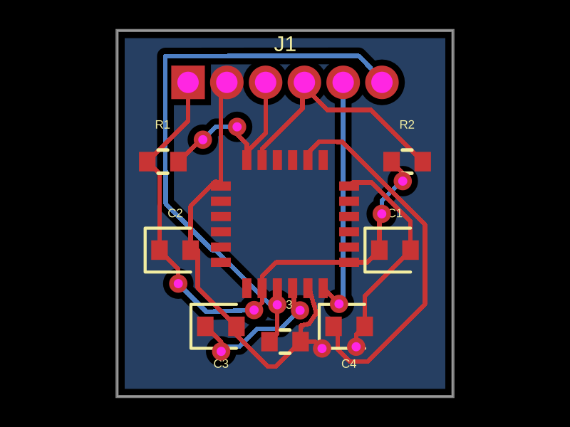
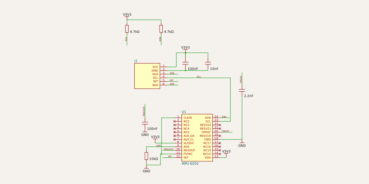
Compact 3.3 V MPU-6050 IMU breakout on an 11×12 mm PCB, with decoupling capacitors, I²C pull-ups, AD0 address pulldown, ground plane, and a 6-pin host header.
- Version
- 1.0.1
- License
- unset
- Stars
- 0
index.circuit.tsx
PCB
Schematic
/** Compact 3.3 V MPU-6050 breakout. J1: 3V3, GND, SDA, SCL, INT, AD0. */
export default () => (
  <board width="11mm" height="12mm" thickness="1.6mm"
    minTraceWidth="0.15mm" nominalTraceWidth="0.15mm"
    minViaHoleDiameter="0.3mm" minViaPadDiameter="0.6mm">
    <copperpour name="GND_PLANE" layer="bottom" connectsTo="net.GND"
      clearance="0.2mm" boardEdgeMargin="0.25mm" />
    <chip
      name="U1"
      manufacturerPartNumber="MPU-6050"
      footprint={
        <footprint>
          <smtpad shape="rect" portHints={["1"]} pcbX={-2.1} pcbY={1.25} width={0.65} height={0.3} />
          <smtpad shape="rect" portHints={["2"]} pcbX={-2.1} pcbY={0.75} width={0.65} height={0.3} />
          <smtpad shape="rect" portHints={["3"]} pcbX={-2.1} pcbY={0.25} width={0.65} height={0.3} />
          <smtpad shape="rect" portHints={["4"]} pcbX={-2.1} pcbY={-0.25} width={0.65} height={0.3} />
          <smtpad shape="rect" portHints={["5"]} pcbX={-2.1} pcbY={-0.75} width={0.65} height={0.3} />
          <smtpad shape="rect" portHints={["6"]} pcbX={-2.1} pcbY={-1.25} width={0.65} height={0.3} />
          <smtpad shape="rect" portHints={["7"]} pcbX={-1.25} pcbY={-2.1} width={0.3} height={0.65} />
          <smtpad shape="rect" portHints={["8"]} pcbX={-0.75} pcbY={-2.1} width={0.3} height={0.65} />
          <smtpad shape="rect" portHints={["9"]} pcbX={-0.25} pcbY={-2.1} width={0.3} height={0.65} />
          <smtpad shape="rect" portHints={["10"]} pcbX={0.25} pcbY={-2.1} width={0.3} height={0.65} />
          <smtpad shape="rect" portHints={["11"]} pcbX={0.75} pcbY={-2.1} width={0.3} height={0.65} />
          <smtpad shape="rect" portHints={["12"]} pcbX={1.25} pcbY={-2.1} width={0.3} height={0.65} />
          <smtpad shape="rect" portHints={["13"]} pcbX={2.1} pcbY={-1.25} width={0.65} height={0.3} />
          <smtpad shape="rect" portHints={["14"]} pcbX={2.1} pcbY={-0.75} width={0.65} height={0.3} />
          <smtpad shape="rect" portHints={["15"]} pcbX={2.1} pcbY={-0.25} width={0.65} height={0.3} />
          <smtpad shape="rect" portHints={["16"]} pcbX={2.1} pcbY={0.25} width={0.65} height={0.3} />
          <smtpad shape="rect" portHints={["17"]} pcbX={2.1} pcbY={0.75} width={0.65} height={0.3} />
          <smtpad shape="rect" portHints={["18"]} pcbX={2.1} pcbY={1.25} width={0.65} height={0.3} />
          <smtpad shape="rect" portHints={["19"]} pcbX={1.25} pcbY={2.1} width={0.3} height={0.65} />
          <smtpad shape="rect" portHints={["20"]} pcbX={0.75} pcbY={2.1} width={0.3} height={0.65} />
          <smtpad shape="rect" portHints={["21"]} pcbX={0.25} pcbY={2.1} width={0.3} height={0.65} />
          <smtpad shape="rect" portHints={["22"]} pcbX={-0.25} pcbY={2.1} width={0.3} height={0.65} />
          <smtpad shape="rect" portHints={["23"]} pcbX={-0.75} pcbY={2.1} width={0.3} height={0.65} />
          <smtpad shape="rect" portHints={["24"]} pcbX={-1.25} pcbY={2.1} width={0.3} height={0.65} />
        </footprint>
      }
      pcbX={0}
      pcbY={-0.35}
      pinLabels={{
        pin1: "CLKIN", pin2: "NC2", pin3: "NC3", pin4: "NC4",
        pin5: "NC5", pin6: "AUX_DA", pin7: "AUX_CL", pin8: "VLOGIC",
        pin9: "AD0", pin10: "REGOUT", pin11: "FSYNC", pin12: "INT",
        pin13: "VDD", pin14: "NC14", pin15: "NC15", pin16: "NC16",
        pin17: "NC17", pin18: "GND", pin19: "RESV19", pin20: "CPOUT",
        pin21: "RESV21", pin22: "RESV22", pin23: "SCL", pin24: "SDA",
      }}
      noConnect={[
        "NC2", "NC3", "NC4", "NC5", "AUX_DA", "AUX_CL",
        "NC14", "NC15", "NC16", "NC17", "RESV19", "RESV21", "RESV22",
      ]}
      connections={{
        CLKIN: "net.GND", VLOGIC: "net.V3V3", AD0: "net.AD0",
        REGOUT: "net.REGOUT", FSYNC: "net.GND", INT: "net.INT",
        VDD: "net.V3V3", GND: "net.GND", CPOUT: "net.CPOUT",
        SCL: "net.SCL", SDA: "net.SDA",
      }}
    />

    <pinheader
      name="J1"
      pinCount={6}
      pitch="1.27mm"
      holeDiameter="0.7mm"
      platedDiameter="1.1mm"
      gender="unpopulated"
      pcbX={0}
      pcbY={4.3}
      pinLabels={{
        pin1: "VCC", pin2: "GND", pin3: "SDA",
        pin4: "SCL", pin5: "INT", pin6: "AD0",
      }}
      connections={{
        VCC: "net.V3V3", GND: "net.GND", SDA: "net.SDA",
        SCL: "net.SCL", INT: "net.INT", AD0: "net.AD0",
      }}
    />

    <capacitor name="C1" capacitance="100nF" footprint="0402" pcbX={3.6} pcbY={-1.2}
      connections={{ pin1: "net.V3V3", pin2: "net.GND" }} />
    <capacitor name="C2" capacitance="10nF" footprint="0402" pcbX={-3.6} pcbY={-1.2}
      connections={{ pin1: "net.V3V3", pin2: "net.GND" }} />
    <capacitor name="C3" capacitance="100nF" footprint="0402" pcbX={-2.1} pcbY={-3.7}
      connections={{ pin1: "net.REGOUT", pin2: "net.GND" }} />
    <capacitor name="C4" capacitance="2.2nF" footprint="0402" pcbX={2.1} pcbY={-3.7}
      connections={{ pin1: "net.CPOUT", pin2: "net.GND" }} />

    <resistor name="R1" resistance="4.7k" footprint="0402" pcbX={-4} pcbY={1.7}
      connections={{ pin1: "net.V3V3", pin2: "net.SDA" }} />
    <resistor name="R2" resistance="4.7k" footprint="0402" pcbX={4} pcbY={1.7}
      connections={{ pin1: "net.V3V3", pin2: "net.SCL" }} />
    <resistor name="R3" resistance="10k" footprint="0402" pcbX={0} pcbY={-4.2}
      connections={{ pin1: "net.AD0", pin2: "net.GND" }} />
  </board>
)
Related Packages
 More from this authorgokul/usb-hub-boardA 4-layer 100×66 mm USB 2.0 hub board with a USB‑C upstream port, four protected downstream USB‑C/USB‑A ports, an integrated SD card reader, USB hub controllers, 3.3 V regulation, ESD protection, current-limited power switches, crystal oscillators, and filtering/passive components.
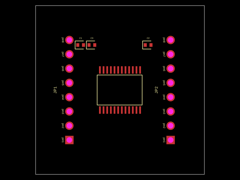 Similar packageimrishabh18/motor-driver-breakout"A 30x30mm TB6612FNG motor driver board with dual 8-pin headers and bypass capacitors for motor control and power regulation"
This summary captures the key physical characteristics:
- Uses TB6612FNG motor driver chip
- 30x30mm board size
- Dual 8-pin headers (JP1 and JP2)
- Includes decoupling capacitors (C1, C2, C3)
- Purpose is motor control and power management
Similar packageimrishabh18/motor-driver-breakout"A 30x30mm TB6612FNG motor driver board with dual 8-pin headers and bypass capacitors for motor control and power regulation"
This summary captures the key physical characteristics:
- Uses TB6612FNG motor driver chip
- 30x30mm board size
- Dual 8-pin headers (JP1 and JP2)
- Includes decoupling capacitors (C1, C2, C3)
- Purpose is motor control and power management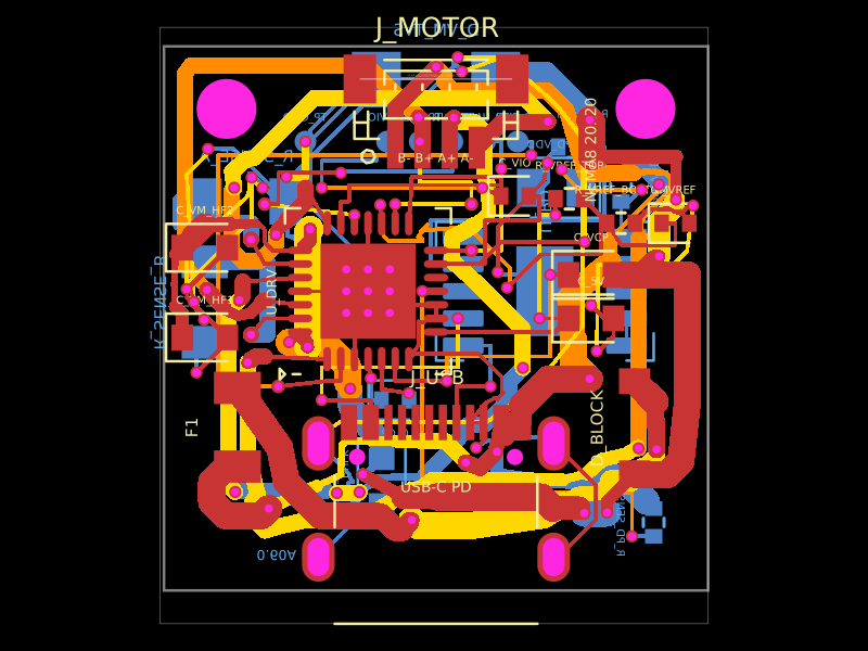 Discover something newShiboSoftwareDev/nema8-20mm-pd-mini-controllerA 20 mm four-layer USB‑C PD 9 V NEMA8 stepper-driver board using CH224K power negotiation/protection and a TMC2209 with current sensing, motor connector, and STEP/DIR/UART control test points.