gokul/lora-device
A compact LoRa/GNSS device PCB integrating an SX1262 radio, GNSS module, USB/UART interface, 1.5 µH inductor, LiPo battery connector with NTC, and supporting passives.
- Version
- 0.1.6
- License
- unset
- Stars
- 0
validation/tscircuit-findings.md
# Reproduced tscircuit findings

## Revision C manufacturing review — 2026-10-22

**New confirmed finding: high impact — overly permissive JLCPCB drill-spacing defaults.** Owning repository: [tscircuit/jlcpcb-manufacturing-specs](https://github.com/tscircuit/jlcpcb-manufacturing-specs/blob/d2fcf9a557a196cf9f2824463d06cd86534b1c21/lib/jlcpcb-manufacturing-specs.ts).

`jlcMinTolerances` sets via-hole edge spacing to 0.10 mm and plated component-hole spacing to 0.15 mm. [JLCPCB's current capability table](https://jlcpcb.com/capabilities/pcb-capabilities) specifies 0.20 mm for via holes and 0.45 mm for pad holes. This is a manufacturing-rule mismatch, not a netlist/short-circuit error.

The real revision-B board had two same-net VBUS vias with only 0.11231 mm between drill edges. `checkSameNetViaSpacing` returned zero errors with its default; with an explicit 0.20 mm requirement it reported that pair. Revision C consolidates the vias and returns zero errors with the stricter requirement. Evidence: `jlc-default-reproduction.json`, `reproductions/jlc-default-spacing.ts.txt` and its minimal input. The current upstream main source was checked at the linked commit; no matching open issue/PR was found during this review. No issue or PR was opened.

Suggested contribution: update the applicable minimum tolerances against the manufacturer table and add a regression case whose gap lies between 0.10 and 0.20 mm. Keep via and component-hole categories distinct. **High impact** here means the defaults can allow an unmanufacturable layout to pass a spacing check; it does not mean every exported board is affected.

Board corrections remain our responsibility. The duplicate drill was caused by almost-coincident authored route coordinates; the small/overlapping silkscreen was our design choice; the USB shell paste followed the existing component-level SMT defaults. Supported source changes resolved these. They are not reported as new upstream defects. The existing 12-section calculation audit found no boundary-correctness bug.

The older findings below are historical reproductions against the dated pinned toolchain. This revision does not claim they were all rechecked against current upstream main.

Rechecked on 2026-10-19 using tscircuit 0.0.2944, core 0.0.2172, CLI 0.1.2365 and TypeScript 5.9.3. These are observed behavior from small reproductions, not inferred from the tracker alone. No GitHub issue or pull request has been opened.

## 1. Schematic grid ignores its prefixed column and gap props

`<group schGrid schGridCols={1} schGridGap={5}>` containing two resistors renders them beside each other at x = −0.8 and +0.8, y = 0. A one-column grid should stack them vertically. The corresponding generic props, `gridCols={1} gridGap={5}`, render them vertically at y = ±2.825.

User impact: the documented schematic-specific grid settings do not control layout, making automatic schematics unexpectedly overlap or wrap. The tracker uses the working generic grid props with `schGrid` enabled.

Evidence: `reproductions/core-reproductions.tsx.txt`, `reproductions/core-results.log` (`grid-prefixed` and `grid-generic`). Suggested contribution scope: resolve schematic-specific grid settings before falling back to generic grid settings; test both prefixed settings and fallback behavior.

## 2. An unbroken board copper pour reserves only the first child group's bounds for routing

A 30 × 20 mm four-layer board containing a small resistor group and a board-level `<copperpour layer="inner1" connectsTo="net.GND" unbroken />` produces an autorouter copper-pour obstacle only 8.45 × 0.95 mm. That is the resistor-group extent, not the board extent.

User impact: signals can be routed on the layer outside that small area even though the author requested a board-wide unbroken ground reference. This can invalidate an intended return-current plane.

Evidence: `plane-board` and `plane-obstacles` in the reproduction results. An otherwise empty first group makes bounds fall back to the board; an explicit full-board outline also works, although its conversion creates many strip obstacles. The final tracker permits signals on inner1 and uses explicit outlines for the local GNSS and USB ground reservations; it does not claim a board-wide unbroken inner1 plane.

Suggested contribution scope: choose the owning board's bounds for a board-level pour, and the owning group's bounds for a group-local pour, rather than choosing the first group in the subcircuit. Include a routing-input regression test with a smaller first child group.

## 3. A schematicbox overlay stays at the pre-layout location

Two chips in an automatically arranged grid put U2 at (2.6, 0). A schematicbox overlay selecting U2's pins remains centered around the old origin: its x extent begins at −1.2 with width 2.4. Its title also remains at the old location.

User impact: an annotation meant to identify a chip can appear over another chip after automatic schematic placement. The tracker uses attached component display text for function and ratings, which follows the chip's final position.

Evidence: `overlay-final-component` and `annotation` in the reproduction results. Suggested contribution scope: regenerate or translate overlay bounds and their title after the selected ports move during layout, including overlays that span multiple pins.

## 4. KiCad conversion emits an unsupported plated-hole prop

Converting KiCad's `JST_PH_B3B-PH-K_1x03_P2.00mm_Vertical.kicad_mod` with the current CLI emits `height` on two `shape="pill"` plated holes. TypeScript rejects both with TS2322 because `PillPlatedHoleProps` has no `height` property. The generated `outerHeight`, `outerWidth`, `holeHeight` and `holeWidth` already specify the geometry.

User impact: newly generated component code cannot pass type checking without manual edits. The tracker's converted connector removes the unsupported prop while retaining the correct pill dimensions.

Reproduce with `bunx tsci convert <KiCad footprint path> --name JstRepro --output JstRepro.tsx`, then run `bunx tsc --noEmit --skipLibCheck --esModuleInterop --jsx react-jsx --moduleResolution node --module ESNext --target ES2020 --types tscircuit JstRepro.tsx`.

Evidence: `reproductions/jst-converted.tsx.txt` and `reproductions/kicad-typecheck.log`. Suggested contribution scope: emit only valid pill-plated-hole attributes, with a generated-source typecheck for a footprint containing oval through-holes.

## 5. Explicit pcbPath layer transitions can lose copper-pour clearance

A two-resistor, two-layer reproduction routes a signal with `pcbPath` entries that include `via: true`, `fromLayer` and `toLayer`, then adds GND pours. The route is drawn through the vias, but adjacent segments are not consistently subtracted from the pours. The default Gerber-based shorts check finds **four signal-to-ground shorts**.

Adding ordinary wire points at the same coordinates immediately before and after each via keeps the physical path unchanged and makes the same check report **zero shorts**. The tracker uses these explicit wire endpoints on all authored layer transitions. Its manual USB paths also pass the Gerber-based shorts check after this change.

User impact: a valid-looking authored trace with layer changes can short to a copper pour in manufacturing output. This finding concerns the geometry around layer transitions, not autorouter route quality.

Evidence: `reproductions/via-path-pour.tsx.txt`, `via-path-implicit-shorts.log` and `via-path-explicit-shorts.log`. Copy the reproduction to a `.tsx` file and run it with Bun once normally and once with `--explicit-wire-points`, then run `tsci check shorts` on each resulting Circuit JSON file. Suggested contribution scope: normalize via-adjacent wire segments consistently before copper-pour generation; test Gerber copper continuity and isolation for both directions of a layer transition.

## 6. Default build discovery rebuilds generated autorouter debug output

In a project with `index.circuit.tsx`, a `mainEntrypoint` config, and `dist/autorouter-debug/board.source-and-pcb.circuit.json`, running plain `tsci build --routing-disabled` reports **two input circuits**. It compiles the debug artifact into `dist/dist/autorouter-debug/board.source-and-pcb/circuit.json` as well as building the real entrypoint.

User impact: a normal build after an autorouter-debug run can compile stale generated board geometry as another project circuit, causing confusing extra outputs and potentially stale diagnostics. The tracker build script explicitly names `index.circuit.tsx`.

Minimal reproduction: create an entrypoint exporting an empty 10 × 10 mm board, set it as `mainEntrypoint`, and create the debug JSON path above containing `[{"type":"pcb_board","pcb_board_id":"pcb_board_0","center":{"x":0,"y":0},"width":10,"height":10,"thickness":1.6,"num_layers":2}]`. Run the command above. Both inputs build successfully, demonstrating input discovery independently of circuit errors.

Evidence: `reproductions/build-discovery.log`. Suggested contribution scope: exclude generated build/debug directories from automatic input discovery, while continuing to accept an explicitly supplied Circuit JSON path. Test a second build after debug output has been generated.

## 7. STEP export rejects valid linked component models with whitespace before the record terminator

A minimal board containing only the exported J1 PCB/CAD records and its linked C165948 STEP model reproduces `Could not parse entity: #1 = DIRECTION ...`. The CLI subsequently reports `Exported to ...` and exits successfully, although it could not merge the connector model. OpenCascade imports that same downloaded file successfully and returns 14 meshes.

The bundled parser matches records with a pattern ending in `\);`; the linked model uses the valid separated form `) ;`. The failure also affected several other linked models in the tracker.

User impact: a mechanical export can omit component geometry while still reporting successful export. The final tracker provides the complete reviewed GLB model; the incomplete STEP export is excluded from the delivery.

Evidence: `reproductions/step-export.circuit.json.txt`, `step-export.log`, and the independent OpenCascade check in `step-model-check.ts.txt` / `step-model-check.log`. Copy the JSON reproduction to `.circuit.json` and run `tsci export <file> -f step -o <absolute-output-path>`. Suggested contribution scope: accept whitespace between the closing parenthesis and semicolon, cover simple and complex entity records, and make unresolved component-model imports explicit in export status.

## 8. Assembly SVG pin-1 marker does not follow a rotated component

A two-chip reproduction places U1 at 0° and U2 at 180°, both with `pin1_location: "leftside_top"` in their authored footprint frame. The placed pad-1 coordinates are upper-left for U1 and lower-right for U2. The assembly SVG draws the dark corner at upper-left for both chips, contradicting U2's physical pad location. The tracker exhibited the same problem on its 180° ESP32 module.

User impact: an assembly drawing can indicate the wrong IC orientation. The delivered drawings instead mark actual pad-1 coordinates obtained from `pcb_port` records, and the corresponding coordinate table is included. The generic assembly SVG is excluded.

Evidence: `reproductions/assembly-pin1.ts.txt`, `assembly-pin1.circuit.json.txt` and the matching SVG/PNG. Run the TypeScript reproduction using circuit-to-svg to compare the two placed chips. Suggested contribution scope: transform pin-1 metadata by component rotation and bottom-side mirroring, or derive the marker from placed pad geometry; cover 0°, 90°, 180° and bottom-side cases.

## 9. Internal chip connections are omitted from the autorouting input

Confirmed on 2026-10-21 with core 0.0.2172 and capacity-autorouter 0.0.988. A reduced version of the tracker's USBLC6 flow-through connection declares two chip pads internally connected and connects a resistor to either side. Core emits the correct `internally_connected_source_port_ids` on the source component, but the Simple Route JSON sent to the autorouter does not preserve that already-connected relationship. Pipeline 9 consequently generates a redundant 4 mm track directly across the two chip pads.

On this tracker, the same behavior produced PCB loops around U6 pins 1–6 and 3–4, including two unnecessary vias on one loop. Those pairs are internally connected in ST's USBLC6-2SC6. Revision B removes both redundant routes and passes source/netlist, PCB DRC and Gerber-short checks.

Affected repository: **tscircuit/core**, `lib/utils/autorouting/getSimpleRouteJsonFromCircuitJson.ts`. The first missing information is in Core's routing input, before the capacity autorouter runs. The existing code populates `externallyConnectedPointIds` from physical PCB traces but does not include the component-internal connection groups. Current main f0a5872fdf24ce15c366c1747574b7b77d4e5829 was inspected and has the same omission; the executable reproduction uses the pinned versions above.

Severity: P2, unnecessary routing and avoidable signal-path loops/vias. Do not describe it as a demonstrated hardware failure. Suggested fix: map valid internally connected source-port groups to PCB point IDs in routing connectivity, preserving them alongside existing physical-route connectivity.

Evidence: `reproductions/internal-connections-repro.tsx.txt`, `internal-connections.routing-input.json.txt`, `internal-connections.circuit.json.txt` and `internal-connections-repro.log`. Related internal-pin PRs were searched; no exact duplicate was identified in that search. No issue or PR has been opened.
Related Packages
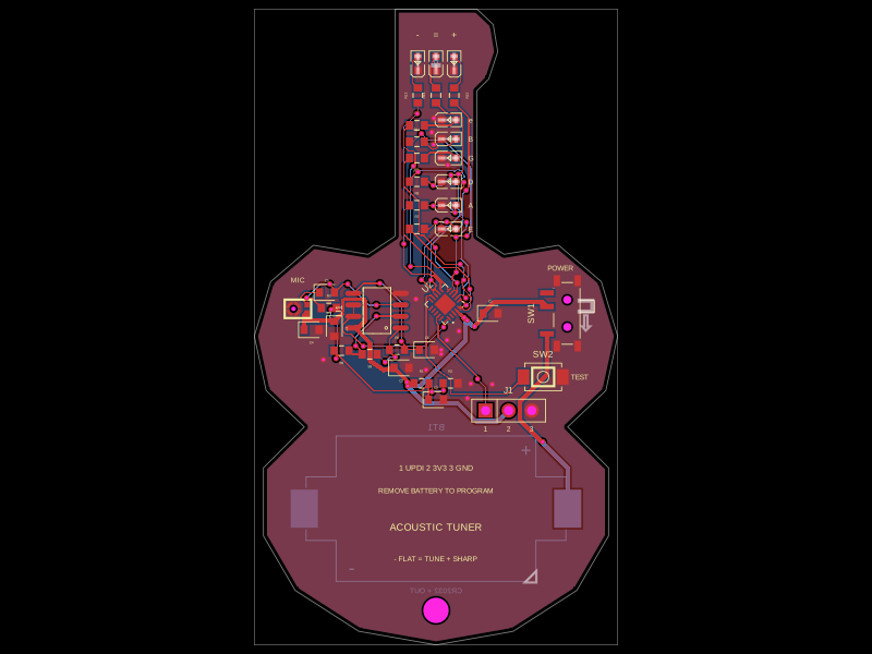 More from this authorgokul/acoustic-guitar-tunerThis code defines the physical pin configuration and footprint layouts for the ATtiny1616 microcontroller and a matching tactile switch component, including their key hardware connection points, dimensions, and 3D models.
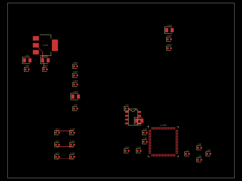 Similar packagecodezonly/pt1This design implements a compact embedded hardware module combining a Seeed XIAO ESP32-C6 microcontroller, a RushFPV GNSS Mini M10 GPS module, and an SX1262 LoRa transceiver, integrated with USB-C power/data, user interface LEDs and buttons, decoupling capacitors, and antenna connectors for GPS and LoRa communication.
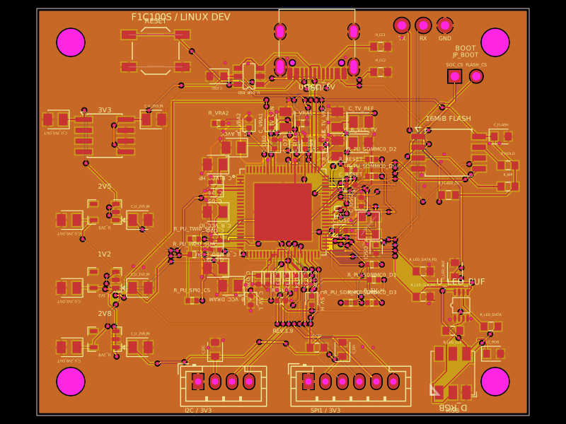 Discover something newseveibar/f1c100s-linux-dev-boardA 4-layer F1C100S Linux development carrier board with USB‑C power/data, multi-rail LDOs, SPI NOR flash, reset/boot interfaces, I²C/SPI/UART headers, ESD protection, and a buffered 5‑V clocked RGB LED.