gokul/lora-device
A compact LoRa/GNSS device PCB integrating an SX1262 radio, GNSS module, USB/UART interface, 1.5 µH inductor, LiPo battery connector with NTC, and supporting passives.
- Version
- 0.1.6
- License
- unset
- Stars
- 0
validation/fabrication-report.md
# Revision C fabrication validation

Reviewed 2026-10-22, package **gokul/lora-device@0.1.6**. The corrected files pass the checks below for a bare-board prototype handoff using **JLCPCB JLC04161H-7628**. The earlier revision-B fabrication-ready statement was too strong: it missed drill-spacing, duplicate-drill and silkscreen problems. Use the revision-C files from this package.

JLCPCB has not accepted this archive through CAM or confirmed its manufactured impedance. No physical board has been assembled or powered. Assembly stock, supplier rotation conventions and prototype bring-up remain outstanding; passing digital checks does not establish those results.

## Design and scope

50 × 78 mm, nominal 1.6 mm, four copper layers, two-sided assembly. 55 fitted references plus three bare test pads. Twelve automatic schematic sections, no schematic sheet wrapper and no authored schX/schY. Existing component positions, copper pads, component holes, source ports/nets/traces and schematic component/trace/section geometry remain unchanged. J2's displayed part number is now complete.

Pinned toolchain: tscircuit 0.0.2944, CLI 0.1.2365, core 0.0.2172, capacity-autorouter 0.0.988, TypeScript 5.9.3. The validated dependencies were retained; this is not a claim that they are the newest npm versions.

## Corrections made

| Prior finding | Revision-C correction |
|---|---|
| VBUS via drill-edge gap 0.11231 mm, below JLCPCB's 0.20 mm requirement | Consolidated the pair into one via and preserved all connected trace paths. |
| Nearly coincident GND vias exported as a duplicate drill hit | Normalized the route coordinates so core emits one physical via. |
| Silkscreen over exposed pads; 0.4 mm labels and 0.036 mm strokes; USB legend outside the board | Replaced footprint clutter with printable functional labels and LED cathode bars. Dense reference designators remain on assembly drawings. |
| Paste over USB shell holes on both sides | Disabled automatic component-wide paste for J1 and defined twelve top-side SMT contact apertures. Shell tabs are soldered separately. |
| Paste on bare test points | Removed TP1–TP3 paste in source. |
| USB nonplated locating-hole copper clearance marginally below 0.20 mm | Added explicit local copper keepouts on all four layers. |
| Optional F_Fab artwork contained zero-width strokes | Excluded optional fabrication artwork from the manufacturing ZIP. |
| J2 unmatched in assembly BOM | Retained the corrected BOM and added exact MPN B3B-PH-K-S(LF)(SN), JLCPCB C131339, to the source. |

The source explicitly enforces 0.20 mm via-hole spacing and 0.45 mm plated component-hole spacing. Revision C has **164 vias and 174 PCB traces**. General routes remain reviewed output from tscircuit's native capacity-autorouter; only local route-coordinate corrections were made. The routing-input hash guard remains enabled and the full build passed.

## Verification results

| Check | Result |
|---|---|
| TypeScript, source, pin specification, netlist, PCB placement, schematic placement | All commands exited successfully; no source/pin/netlist errors. |
| Full guarded build | 2,675 Circuit JSON records; zero error records. |
| All-layer Gerber-mode short check and PCB routing-style check | Passed. |
| Independent exported-Gerber connectivity | 42 logical groups / 215 connected component pins; zero missing pad connections, opens or shorts. Includes declared internal IC connections. |
| Drill export | 171 plated features: 164 vias, 3 J2 holes, 4 USB shell slots; 2 NPTH locating holes. No duplicate hits. |
| Closest drill-edge separation | 0.44994 mm, between vias; exceeds their 0.20 mm requirement. Component-hole spacing also passes the explicit 0.45 mm source rule. |
| Copper to routed board edge | At least 0.32587 mm; no copper outside the outline. |
| NPTH to copper | At least 0.20767 mm. |
| Hole to copper on other connected nets | Via minimum 0.29932 mm; component-hole minimum 0.425 mm. Passes the applicable 0.20 / 0.28 / 0.30 mm checks. |
| Annular ring | Nominal 0.15 mm; polygon approximation gives 0.14992 mm, within the 0.0001 mm numerical allowance. |
| Outer-layer separate copper gaps | At least 0.14932 mm. No distinct connected-net gaps below 0.10 mm found on any layer. |
| Solder-mask bridges | Top minimum 0.19962 mm; bottom 0.15 mm. |
| Silkscreen | No mask-opening overlaps or off-board ink. Top minimum mask clearance 0.18887 mm; bottom 1.98534 mm. Minimum stroke 0.20 mm. |
| Solder paste | No paste outside copper/mask, over plated holes, or on TP1–TP3. |
| USB main pair | Width 0.24 mm, coupled gap 0.16 mm; unchanged 0.68279 mm planar mismatch. Checked bottom-path centerlines have no uncovered inner2 reference outside via-antipad exclusions. |
| BOM / placements | Same 55 fitted references; J2 mapping verified; native placement CSV byte-identical to the previous release. |
| Views | PCB top/bottom and both inner layers, thirteen Gerber/drill layers, schematic SVG/PNG/PDF, actual-pad assembly drawings and 3D top/bottom/side reviewed. |

The independent Gerber audit uses Gerbonara 0.13.0 and Shapely 2.2.0. Drill G85 slot endpoints are parsed explicitly; the generic parser's unsupported-slot warning is not treated as a bad drill file. Circular geometry is polygonally approximated, so reported figures are design checks, not finished-board measurements. Three inner2 same-ground islands touch at via-pad edges; they belong to the same connected GND network through other layers and are not shorts or different-net spacing violations.

Evidence: `rev-c-check-results.json`, `rev-c-change-audit.json`, `rev-c-gerber-geometry.json`, `rev-c-gerber-clearances.json`, `rev-c-gerber-connectivity.json`, `rev-c-silkscreen.json`, the `rev-c-*.log` files, and `jlcpcb-usb-geometry.json`.

## USB stack-up and retained warnings

Use JLC04161H-7628, 1 oz outer / 0.5 oz inner copper, nominal 1.6 mm. The official calculator previously returned 0.2383 mm width at 90 Ω for the selected geometry; the authored main run is rounded to 0.24 mm with 0.16 mm pair gap and 0.20 mm adjacent ground clearance. Request **90 Ω ±10%** and obtain JLCPCB's CAM acceptance and impedance report. See `docs/jlcpcb-fabrication.md` and `jlcpcb-calculator.png`.

The build retains the intentional missing-sheet warning and two width warnings for short 0.20 mm USB escapes on nets whose main paths are 0.24 mm. The escapes, component pads, ESD device and vias are local impedance discontinuities. No complete-channel simulation or USB compliance test is claimed. The geometry check verifies the selected layout, not the impedance of a manufactured board.

## Manufacturing and assembly handoff

Bare-board authority: `dist/manufacturing/gerbers.zip`, containing **13 Gerber/drill files**. SHA-256: `b939d597e18d29308a69a9d780f811d77162d2a82694563877bff81a04086110`.

Complete handoff: `dist/manufacturing/lora-device-rev-c.zip`. It includes fabrication outputs, BOM, native placements, assembly drawings, schematic, instructions and current validation records. Source, 3D assets and the KiCad reference are available separately in the same package. Do not upload the older revision-B archive.

Use `dist/assembly/bom.csv` and `placements-native.csv` with the actual pad-1/cathode drawings and `docs/assembly-orientation.md`. J2 and J1's shell tabs need through-hole/selective or hand soldering; only J1's SMT contacts receive stencil paste. The board needs both-side SMT assembly. The BOM still has 42 entries without explicit supplier codes, relying on exact-MPN matching. A part number does not guarantee current stock; the shortages shown in the earlier order screenshot cannot be resolved by Gerber changes. Supplier feeder rotations remain unverified and require assembly preview approval.

The battery, external LoRa antenna, gateway and application firmware are not included. Follow the current-limited first-power procedure in `docs/assembly.md`, then test USB enumeration, charging, supply transients, temperature, GNSS reception and LoRa operation on the first sample.

## CAD and upstream findings

The 20 manufacturer-derived model assets remain unchanged; the other 35 models are still library/nominal geometry. All 55 fitted components are present in the GLB. Complete manufacturer-CAD coverage and enclosure-fit qualification remain unfinished; see `docs/manufacturer-models.md`. The exported KiCad archive is an editable reference with unverified STEP exports removed, not an independently KiCad-DRC-qualified fabrication authority.

One new genuine upstream finding was confirmed: **tscircuit/jlcpcb-manufacturing-specs uses overly permissive drill-spacing defaults**. The old 0.11231 mm VBUS gap passes the default same-net-via check but fails with JLCPCB's 0.20 mm threshold. Revision C overrides the defaults and fixes the geometry. See `tscircuit-findings.md` and the runnable five-record reproduction. No GitHub issue or PR was opened. The earlier findings remain dated historical evidence; no new calculate-cell-boundaries defect was found.
Related Packages
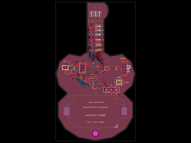 More from this authorgokul/acoustic-guitar-tunerThis code defines the physical pin configuration and footprint layouts for the ATtiny1616 microcontroller and a matching tactile switch component, including their key hardware connection points, dimensions, and 3D models.
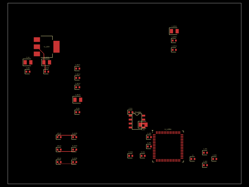 Similar packagecodezonly/pt1This design implements a compact embedded hardware module combining a Seeed XIAO ESP32-C6 microcontroller, a RushFPV GNSS Mini M10 GPS module, and an SX1262 LoRa transceiver, integrated with USB-C power/data, user interface LEDs and buttons, decoupling capacitors, and antenna connectors for GPS and LoRa communication.
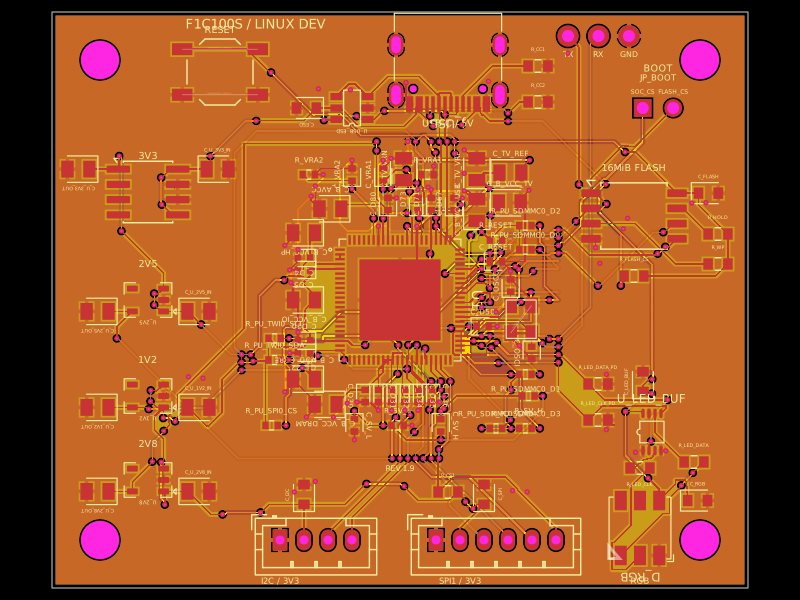 Discover something newseveibar/f1c100s-linux-dev-boardA 4-layer F1C100S Linux development carrier board with USB‑C power/data, multi-rail LDOs, SPI NOR flash, reset/boot interfaces, I²C/SPI/UART headers, ESD protection, and a buffered 5‑V clocked RGB LED.