gokul/lora-device
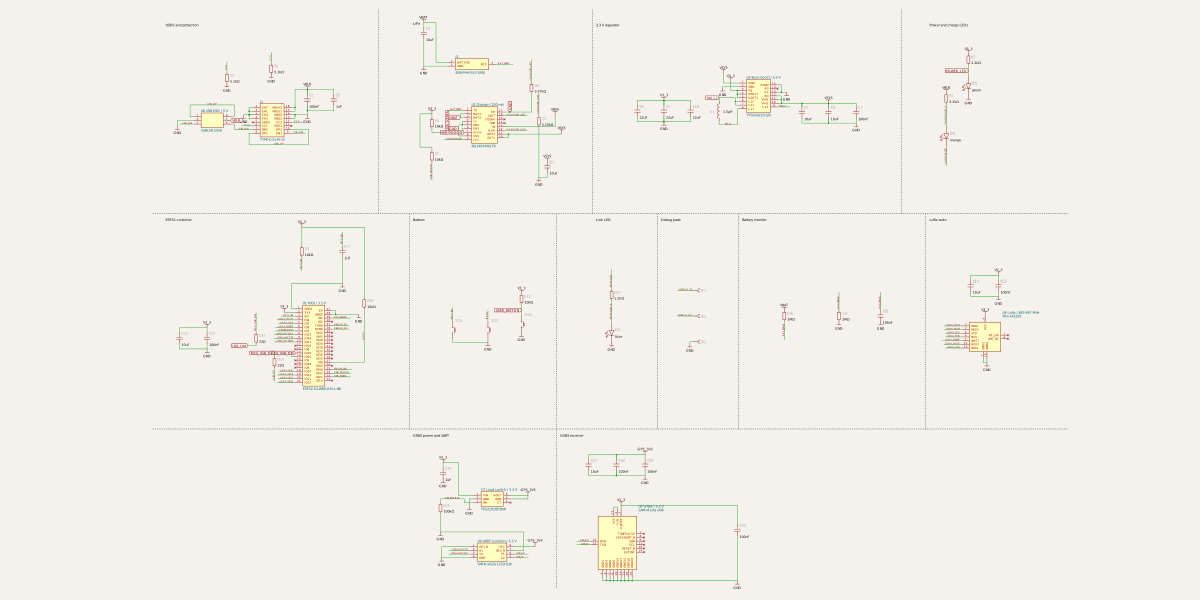
A compact LoRa/GNSS device PCB integrating an SX1262 radio, GNSS module, USB/UART interface, 1.5 µH inductor, LiPo battery connector with NTC, and supporting passives.
- Version
- 0.1.6
- License
- unset
- Stars
- 0
index.circuit.tsx
PCB
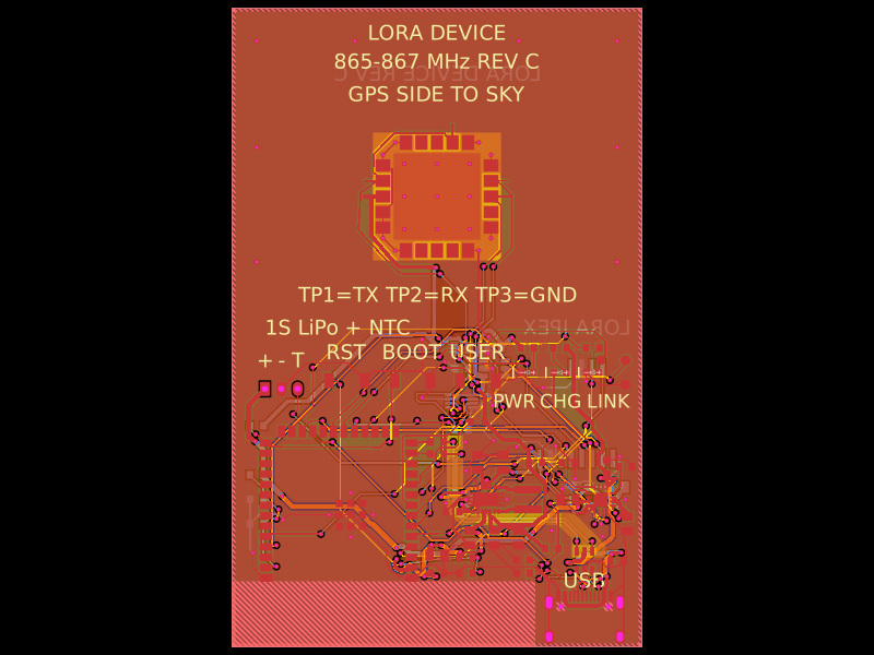
Schematic
import { createTrackerAutorouter } from "./routing/autorouter";
import { PowerSection } from "./sections/PowerSection";
import { ControllerSection } from "./sections/ControllerSection";
import { RadioGnssSection } from "./sections/RadioGnssSection";
import { BoardLegend } from "./components/BoardLegend";
import { UsbRouting } from "./components/UsbRouting";

export default function IndiaLoRaTracker() {
  return (
    <board
      title="lora-device"
      width={50}
      height={78}
      thickness={1.6}
      layers={4}
      doubleSidedAssembly
      autorouter={{ preset: "auto_local", traceClearance: 0.2 }}
      autorouterVersion="beta_pipeline9"
      routeRemaining={false}
      autorouterEffortLevel="5x"
      minTraceWidth={0.2}
      defaultTraceWidth={0.2}
      minTraceToPadEdgeClearance={0.15}
      minViaEdgeToPadEdgeClearance={0.25}
      minPadEdgeToPadEdgeClearance={0.15}
      minViaHoleEdgeToViaHoleEdgeClearance={0.2}
      minPlatedHoleDrillEdgeToDrillEdgeClearance={0.45}
      minViaHoleDiameter={0.3}
      minViaPadDiameter={0.6}
      pcbStyle={{ viaPadDiameter: 0.6, viaHoleDiameter: 0.3 }}
      minBoardEdgeClearance={0.3}
      allowBlindAndBuriedVias={false}
      defaultViaTenting="both_sides"
      schAutoLayoutEnabled
      schTraceAutoLabelEnabled
      schMaxTraceDistance={2}
    >
      <net name="GND" isGroundNet routingPhaseIndex={0} />
      <net
        name="VBUS"
        routingPhaseIndex={0}
        isPowerNet
        nominalTraceWidth={0.5}
      />
      <net
        name="VBAT"
        routingPhaseIndex={0}
        isPowerNet
        nominalTraceWidth={0.6}
      />
      <net
        name="VSYS"
        routingPhaseIndex={0}
        isPowerNet
        nominalTraceWidth={0.4}
      />
      <net
        name="V3_3"
        routingPhaseIndex={0}
        isPowerNet
        nominalTraceWidth={0.5}
      />
      <net name="SW_L1" nominalTraceWidth={0.5} />
      <net name="SW_L2" nominalTraceWidth={0.5} />
      <net
        name="GPS_3V3"
        routingPhaseIndex={0}
        isPowerNet
        nominalTraceWidth={0.3}
      />
      <net name="CC1" routingPhaseIndex={0} />
      <net name="CC2" routingPhaseIndex={0} />
      <net name="USB_DP" routingPhaseIndex={0} />
      <net name="USB_DM" routingPhaseIndex={0} />
      <net name="BAT_TEMP" routingPhaseIndex={0} />
      <net name="USB_500MA" routingPhaseIndex={0} />
      <net name="USB_PGOOD" routingPhaseIndex={0} />
      <net name="CHARGE_LED" routingPhaseIndex={0} />
      <net name="CHARGER_ILIM" routingPhaseIndex={0} />
      <net name="CHARGER_ISET" routingPhaseIndex={0} />
      <net name="POWER_LED" routingPhaseIndex={0} />
      <net name="CHARGE_LED_A" routingPhaseIndex={0} />
      <net name="MCU_EN" routingPhaseIndex={0} />
      <net name="BOOT" routingPhaseIndex={0} />
      <net name="LORA_NSS" routingPhaseIndex={0} />
      <net name="LORA_MOSI" routingPhaseIndex={0} />
      <net name="LORA_SCK" routingPhaseIndex={0} />
      <net name="LORA_MISO" routingPhaseIndex={0} />
      <net name="LORA_BUSY" routingPhaseIndex={0} />
      <net name="LORA_IRQ" routingPhaseIndex={0} />
      <net name="LORA_RESET" routingPhaseIndex={0} />
      <net name="GPS_ENABLE" routingPhaseIndex={0} />
      <net name="GPS_UART_RX" routingPhaseIndex={0} />
      <net name="GPS_UART_TX" routingPhaseIndex={0} />
      <net name="USER_BUTTON" routingPhaseIndex={0} />
      <net name="STATUS_LED" routingPhaseIndex={0} />
      <net name="BAT_SENSE" routingPhaseIndex={0} />
      <net name="DEBUG_TX" routingPhaseIndex={0} />
      <net name="DEBUG_RX" routingPhaseIndex={0} />
      <net name="STATUS_LED_A" routingPhaseIndex={0} />
      <net name="GPS_RX" routingPhaseIndex={0} />
      <net name="GPS_TX" routingPhaseIndex={0} />
      <group name="GroundPlane">
        <copperpour
          name="GroundReference"
          layer="inner1"
          connectsTo="net.GND"
          clearance={0.2}
          boardEdgeMargin={0.3}
        />
      </group>
      <autoroutingphase
        name="SignalsAndPower"
        phaseIndex={0}
        algorithmFn={createTrackerAutorouter}
        autorouter="auto_local"
      />
      <UsbRouting />
      <BoardLegend />
      {/* Give the USB locating holes 0.25 mm copper clearance, including polygon approximation. */}
      <keepout shape="rect" pcbX={15.100082} pcbY={-34.0944328} width={1.1} height={1.1} layers={["top", "inner1", "inner2", "bottom"]} excludeRefs={[".J1"]} />
      <keepout shape="rect" pcbX={20.899918} pcbY={-34.0944328} width={1.1} height={1.1} layers={["top", "inner1", "inner2", "bottom"]} excludeRefs={[".J1"]} />
      <group
        name="TrackerSchematic"
        pcbX={0}
        pcbY={0}
        pcbRelative
        schAutoLayoutEnabled
      >
        <PowerSection />
        <ControllerSection />
        <RadioGnssSection />
      </group>
      <schematicsection name="Usb" displayName="USB-C and protection" />
      <schematicsection name="Charger" displayName="LiPo" />
      <schematicsection name="Regulator" displayName="3.3 V regulator" />
      <schematicsection
        name="PowerIndicators"
        displayName="Power and charge LEDs"
      />
      <schematicsection name="Mcu" displayName="ESP32 controller" />
      <schematicsection name="Controls" displayName="Buttons" />
      <schematicsection name="LinkLed" displayName="Link LED" />
      <schematicsection name="Debug" displayName="Debug pads" />
      <schematicsection name="BatteryMonitor" displayName="Battery monitor" />
      <schematicsection name="LoRa" displayName="LoRa radio" />
      <schematicsection name="GnssPower" displayName="GNSS power and UART" />
      <schematicsection name="GnssReceiver" displayName="GNSS receiver" />
      <copperpour
        name="GnssTopReference"
        layer="top"
        connectsTo="net.GND"
        unbroken
        outline={[
          { x: -5.5, y: 10.5 },
          { x: 5.5, y: 10.5 },
          { x: 5.5, y: 21.5 },
          { x: -5.5, y: 21.5 },
        ]}
        clearance={0.2}
      />
      <copperpour
        name="BottomGround"
        layer="bottom"
        connectsTo="net.GND"
        clearance={0.2}
        boardEdgeMargin={0.3}
      />
      <copperpour
        name="TopGround"
        layer="top"
        connectsTo="net.GND"
        clearance={0.2}
        boardEdgeMargin={0.3}
      />
      <keepout
        shape="rect"
        pcbX={-6.5}
        pcbY={-35}
        width={37}
        height={8}
        layers={["top", "inner1", "inner2", "bottom"]}
        excludeRefs={[".U1"]}
      />
      <copperpour
        name="GnssInner1Ground"
        layer="inner1"
        connectsTo="net.GND"
        unbroken
        outline={[
          { x: -8, y: 8 },
          { x: 8, y: 8 },
          { x: 8, y: 24 },
          { x: -8, y: 24 },
        ]}
        clearance={0.2}
      />
      <copperpour
        name="GnssInnerGround"
        layer="inner2"
        connectsTo="net.GND"
        unbroken
        outline={[
          { x: -8, y: 8 },
          { x: 8, y: 8 },
          { x: 8, y: 24 },
          { x: -8, y: 24 },
        ]}
        clearance={0.2}
      />
      <copperpour
        name="GnssBottomGround"
        layer="bottom"
        connectsTo="net.GND"
        unbroken
        outline={[
          { x: -8, y: 8 },
          { x: 8, y: 8 },
          { x: 8, y: 24 },
          { x: -8, y: 24 },
        ]}
        clearance={0.2}
      />
      <via
        name="GndStitch1"
        connectsTo="net.GND"
        pcbX={3.5}
        pcbY={-21}
        outerDiameter={0.6}
        holeDiameter={0.3}
        layers={["top", "bottom"]}
      />
      <via
        name="GndStitch2"
        connectsTo="net.GND"
        pcbX={8.5}
        pcbY={-21}
        outerDiameter={0.6}
        holeDiameter={0.3}
        layers={["top", "bottom"]}
      />
      <via
        name="GndStitch3"
        connectsTo="net.GND"
        pcbX={23}
        pcbY={-21}
        outerDiameter={0.6}
        holeDiameter={0.3}
        layers={["top", "bottom"]}
      />
      <via
        name="GndStitch4"
        connectsTo="net.GND"
        pcbX={20}
        pcbY={-24}
        outerDiameter={0.6}
        holeDiameter={0.3}
        layers={["top", "bottom"]}
      />
      <via
        name="GndStitch5"
        connectsTo="net.GND"
        pcbX={-22}
        pcbY={8}
        outerDiameter={0.6}
        holeDiameter={0.3}
        layers={["top", "bottom"]}
      />
      <via
        name="GndStitch6"
        connectsTo="net.GND"
        pcbX={-22}
        pcbY={22}
        outerDiameter={0.6}
        holeDiameter={0.3}
        layers={["top", "bottom"]}
      />
      <via
        name="GndStitch7"
        connectsTo="net.GND"
        pcbX={-22}
        pcbY={35}
        outerDiameter={0.6}
        holeDiameter={0.3}
        layers={["top", "bottom"]}
      />
      <via
        name="GndStitch8"
        connectsTo="net.GND"
        pcbX={22}
        pcbY={8}
        outerDiameter={0.6}
        holeDiameter={0.3}
        layers={["top", "bottom"]}
      />
      <via
        name="GndStitch9"
        connectsTo="net.GND"
        pcbX={22}
        pcbY={22}
        outerDiameter={0.6}
        holeDiameter={0.3}
        layers={["top", "bottom"]}
      />
      <via
        name="GndStitch10"
        connectsTo="net.GND"
        pcbX={22}
        pcbY={35}
        outerDiameter={0.6}
        holeDiameter={0.3}
        layers={["top", "bottom"]}
      />
      <via
        name="GndStitch11"
        connectsTo="net.GND"
        pcbX={-10}
        pcbY={35}
        outerDiameter={0.6}
        holeDiameter={0.3}
        layers={["top", "bottom"]}
      />
      <via
        name="GndStitch12"
        connectsTo="net.GND"
        pcbX={10}
        pcbY={35}
        outerDiameter={0.6}
        holeDiameter={0.3}
        layers={["top", "bottom"]}
      />
      <keepout
        shape="rect"
        pcbX={-24.8}
        pcbY={0}
        width={0.4}
        height={78}
        layers={["top", "inner1", "inner2", "bottom"]}
      />
      <keepout
        shape="rect"
        pcbX={24.8}
        pcbY={0}
        width={0.4}
        height={78}
        layers={["top", "inner1", "inner2", "bottom"]}
      />
      <keepout
        shape="rect"
        pcbX={0}
        pcbY={38.8}
        width={50}
        height={0.4}
        layers={["top", "inner1", "inner2", "bottom"]}
      />
      <keepout
        shape="rect"
        pcbX={0}
        pcbY={-38.8}
        width={50}
        height={0.4}
        layers={["top", "inner1", "inner2", "bottom"]}
        excludeRefs={[".J1"]}
      />
    </board>
  );
}
Related Packages
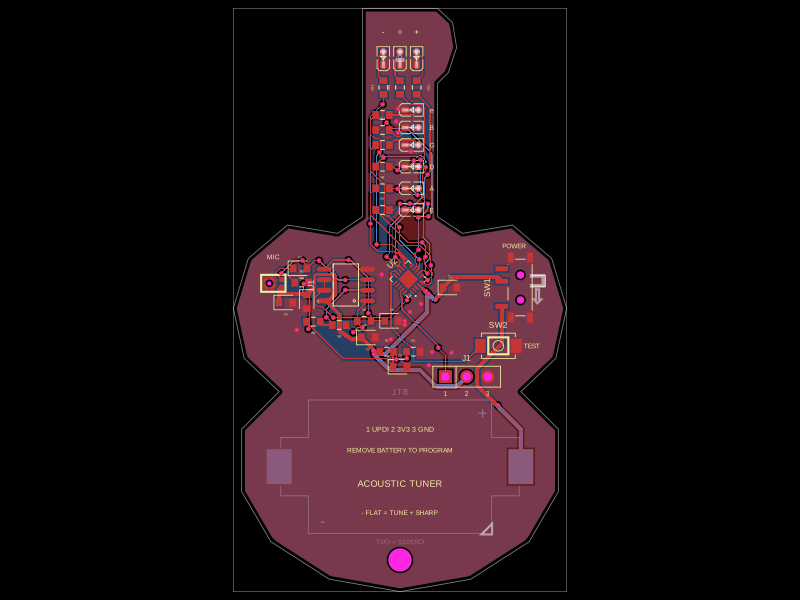 More from this authorgokul/acoustic-guitar-tunerThis code defines the physical pin configuration and footprint layouts for the ATtiny1616 microcontroller and a matching tactile switch component, including their key hardware connection points, dimensions, and 3D models.
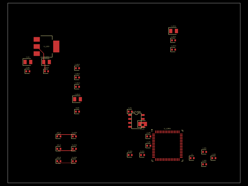 Similar packagecodezonly/pt1This design implements a compact embedded hardware module combining a Seeed XIAO ESP32-C6 microcontroller, a RushFPV GNSS Mini M10 GPS module, and an SX1262 LoRa transceiver, integrated with USB-C power/data, user interface LEDs and buttons, decoupling capacitors, and antenna connectors for GPS and LoRa communication.
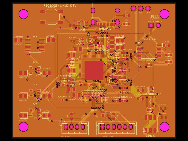 Discover something newseveibar/f1c100s-linux-dev-boardA 4-layer F1C100S Linux development carrier board with USB‑C power/data, multi-rail LDOs, SPI NOR flash, reset/boot interfaces, I²C/SPI/UART headers, ESD protection, and a buffered 5‑V clocked RGB LED.