gokul/lora-device
A compact LoRa/GNSS device PCB integrating an SX1262 radio, GNSS module, USB/UART interface, 1.5 µH inductor, LiPo battery connector with NTC, and supporting passives.
- Version
- 0.1.6
- License
- unset
- Stars
- 0
docs/jlcpcb-fabrication.md
# Revision C — JLCPCB fabrication specification

Updated 2026-10-22 for package v0.1.6. These are bare-board fabrication instructions. Use the 13-file revision-C Gerber/drill ZIP. No order has been submitted and JLCPCB has not reviewed this particular Gerber archive. A first prototype still needs electrical bring-up.

## Order settings

| Setting | Requirement |
|---|---|
| Board | 50 × 78 mm, four layers, nominal 1.6 mm FR-4 |
| Stack-up | **JLC04161H-7628**, the standard 1.6 mm option; do not substitute 3313/1080 |
| Outer copper | 1 oz, 0.035 mm finished in the published calculator model |
| Inner copper | 0.5 oz, 0.0152 mm in the published calculator model |
| Surface finish / mask | ENIG / green solder mask, both sides |
| Impedance control | Yes; USB differential pair **90 Ω ±10%** |
| USB signal / reference | L4 (bottom) / L3 (inner2) GND |
| Main pair geometry | 0.24 mm width, 0.16 mm edge-to-edge spacing, 0.20 mm adjacent ground clearance |
| Vias | Plated through; nominal 0.30 mm finished hole / 0.60 mm pad; no blind or buried vias |
| Assembly | Components on both sides; J2 through-hole. Order assembly separately after BOM/rotation review. |

JLCPCB's calculator identifies this stack-up as a finished thickness of about 1.59 mm ±10%, under its nominal 1.6 mm ordering option. The layer schedule is:

| Layer / dielectric | Thickness |
|---|---:|
| L1 top copper | 0.0350 mm |
| 7628 prepreg (published Dk 4.4) | 0.2104 mm |
| L2 / inner1 copper | 0.0152 mm |
| Core | 1.0650 mm |
| L3 / inner2 copper | 0.0152 mm |
| 7628 prepreg | 0.2104 mm |
| L4 bottom copper | 0.0350 mm |

Use the named manufacturer stack-up, rather than treating the nominal 1.6 mm as an exact sum of these modeled layer thicknesses.

## USB calculation and layout check

The official JLCPCB calculator was set to four layers, 1.6 mm, 1 oz outer / 0.5 oz inner copper, millimeters, coplanar differential pair with solder mask, L4 signal / L3 reference, 90 Ω, 0.16 mm pair spacing and 0.20 mm ground gap. For JLC04161H-7628 it returned **0.2383 mm track width**, rounded to **0.24 mm** in this layout. The calculator's displayed ±0.5% is its numerical search tolerance; the fabrication acceptance requirement is **±10%**, not ±0.5%.

Evidence: `validation/jlcpcb-calculator.png` and `validation/jlcpcb-usb-geometry.json`.

The main parallel run is 0.24 mm wide with a 0.16 mm gap, including the corrected 45° bend. Its L3 ground reference is continuous along the bottom-layer centerlines outside the normal signal-via antipads. Four existing nearby GND vias connect the reference to the outer ground pours. The planar U6-to-series-resistor lengths are 27.9271 mm (D+) and 28.6099 mm (D−), a 0.6828 mm difference. These figures exclude via barrel length and connector-side fan-outs.

The short connector escapes and MCU pin escapes remain 0.20 mm wide to meet local pad/via clearances. They, component pads, the protection chip and via transitions are localized impedance discontinuities; they are not modeled as uniform 90 Ω lines. The complete USB channel has not been field-simulated or physically measured. This is the ESP32-S3's full-speed USB interface, not a qualified high-speed USB 480 Mb/s design.

Two redundant PCB connections across U6 pin 1–6 and pin 3–4 were removed. Those pairs are internally connected by the USBLC6-2SC6 itself. The remaining routing passes the connectivity and shorts checks.

## Fabricator note — include with the order

> Fabricate lora-device REV C using JLC04161H-7628, nominal 1.6 mm, four layers, 1 oz outer / 0.5 oz inner copper, ENIG and green solder mask. Control the bottom-layer USB main differential pair to 90 Ω ±10%, referenced to the inner2/L3 GND region. Main geometry is W=0.24 mm, pair gap=0.16 mm, adjacent same-layer GND gap=0.20 mm. Preserve the short 0.20 mm component escapes, antenna copper exclusion and reference-ground regions. Use the supplied Gerbers and drill files as manufacturing authority. Please report any required CAM change to the stack-up, trace widths or pair spacing before production. Include the impedance test result/coupon report with the order.

That CAM review is a normal fabricator handoff. Do not substitute a different stack-up or manufacture the older revision-A Gerbers with these settings.

## Revision C manufacturing checks

The corrected export has 164 distinct vias, seven plated component holes/slots and two nonplated USB locating holes. Closest hole-edge separation is approximately 0.44994 mm; this closest pair is vias, above their 0.20 mm requirement. Copper remains at least 0.32587 mm from the routed outline. Minimum USB NPTH-to-copper clearance is 0.20767 mm. Plated annular ring is nominally 0.15 mm; the polygon approximation measures 0.14992 mm. These are the exported design values, not measurements of a finished board.

Source rules explicitly set 0.20 mm via-hole spacing and 0.45 mm component-hole spacing. See the validation report and actual Gerber audit for applicability and numerical precision. Optional F_Fab artwork and unverified automatic BOM/PnP files are excluded from the fabrication ZIP.

## References

- [JLCPCB impedance calculator](https://jlcpcb.com/pcb-impedance-calculator)
- [JLCPCB stack-ups and dielectric parameters](https://jlcpcb.com/impedance)
- [Espressif ESP32-S3 USB layout guidance](https://docs.espressif.com/projects/esp-hardware-design-guidelines/en/latest/esp32s3/pcb-layout-design.html#usb)
- [ST USBLC6-2 datasheet, functional diagram](https://www.st.com/resource/en/datasheet/usblc6-2.pdf)
Related Packages
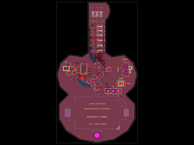 More from this authorgokul/acoustic-guitar-tunerThis code defines the physical pin configuration and footprint layouts for the ATtiny1616 microcontroller and a matching tactile switch component, including their key hardware connection points, dimensions, and 3D models.
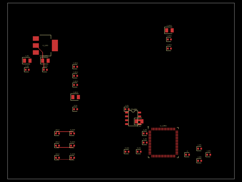 Similar packagecodezonly/pt1This design implements a compact embedded hardware module combining a Seeed XIAO ESP32-C6 microcontroller, a RushFPV GNSS Mini M10 GPS module, and an SX1262 LoRa transceiver, integrated with USB-C power/data, user interface LEDs and buttons, decoupling capacitors, and antenna connectors for GPS and LoRa communication.
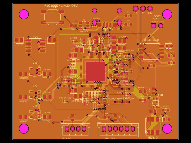 Discover something newseveibar/f1c100s-linux-dev-boardA 4-layer F1C100S Linux development carrier board with USB‑C power/data, multi-rail LDOs, SPI NOR flash, reset/boot interfaces, I²C/SPI/UART headers, ESD protection, and a buffered 5‑V clocked RGB LED.