gokul/lora-device
A compact LoRa/GNSS device PCB integrating an SX1262 radio, GNSS module, USB/UART interface, 1.5 µH inductor, LiPo battery connector with NTC, and supporting passives.
- Version
- 0.1.6
- License
- unset
- Stars
- 0
docs/assembly.md
# Assembly and fabrication notes

Use the revision-C manufacturing archive named in the validation report. Development and failed exports have been removed from the delivery directory.

## PCB

- Outline: 50 × 78 mm; finished thickness 1.6 mm; four copper layers.
- Two-sided SMT assembly, with J2 as a through-hole connector. USB shell tabs are also plated through-hole features. No blind or buried vias. Nominal routed vias use 0.30 mm finished holes and 0.60 mm copper pads, tented on both outer sides.
- Minimum authored signal width 0.20 mm; copper clearance target at least 0.15 mm; board-edge copper clearance at least 0.30 mm. Fine-pitch IC pads follow their package land patterns.
- Use JLCPCB **JLC04161H-7628**, 1 oz outer / 0.5 oz inner copper, nominal 1.6 mm. USB D+/D− use 0.24 mm width and 0.16 mm edge spacing along the bottom-layer main run over the inner2/L3 GND region, with 0.20 mm adjacent ground clearance. Request 90 Ω ±10% impedance control. Short component escapes remain 0.20 mm. See `jlcpcb-fabrication.md` for calculator evidence, the complete layer schedule and the order note.
- Preserve the ESP32 antenna copper exclusion and the GNSS ground areas. Do not add copper, mounting screws, metal enclosure features or a battery in the ESP32 antenna exclusion.
- Keep the enclosure at least 5 mm above the GNSS patch and avoid nearby metal. The radio's antenna connector needs cable access below the PCB.

The stencil files intentionally exclude the four USB shell slots, J2 holes and TP1–TP3. Apply paste to the USB SMT signal contacts using the supplied top stencil; solder the shell tabs and J2 separately by a suitable selective/hand process. Do not assume pin-in-paste reflow for the shell. Both sides contain SMT parts.

Revision C uses legible functional silkscreen labels and LED cathode bars. Dense component reference designators are supplied in the assembly drawings; they are deliberately omitted from the board silkscreen to maintain pad clearance and printable stroke widths.

## Parts and polarity

Use the exact manufacturer part numbers in the BOM. A supplier number is a sourcing aid; it does not authorize substituting a different footprint or electrical rating.

U4 must be the IPEX-connector Wio-SX1262, Seeed SKU 114993390. Its `ANT_NC` pad is intentionally unused. The manufacturer-published radio model includes its onboard connector but not the attached cable.

J2 is JST B3B-PH-K-S(LF)(SN), JLCPCB C131339: pin 1 BAT+, pin 2 GND, pin 3 battery NTC. Use a protected 1S LiPo with a 10 kΩ, Semitec 103AT-2-compatible thermistor and a charge-current rating of at least 250 mA. Check the cable pin order explicitly.

D1 is green PWR, D2 amber CHG, D3 blue LINK. Confirm cathode orientation against the footprint pad labels and the assembly drawing. Use the pin-1 marks for U1–U8. The three test pads TP1–TP3 have no fitted components.

Use the supplied `placements-native.csv` and `assembly-orientation.md`. The bottom assembly drawing is viewed from below, with X mirrored; CSV coordinates remain in the common top-view board coordinate system. A generic placement angle is not a universal feeder angle. The assembler must reconcile polarized parts and IC pin 1 with the board's pad numbers and the assembly drawing. Bottom-side coordinates and rotation conventions must match the assembler's import settings.

## Initial power-up

Start with a current-limited 5 V supply and no battery. Check for rail-to-ground shorts, then verify 3.3 V before attaching a battery. The green LED should light. Confirm native USB enumeration before loading firmware. Inspect charger temperature and verify approximately 250 mA charging with the intended battery and thermistor.

Hardware measurements remain necessary for antenna performance, GNSS reception, USB signal integrity, supply transients and thermal behavior. No physical prototype has yet been tested.
Related Packages
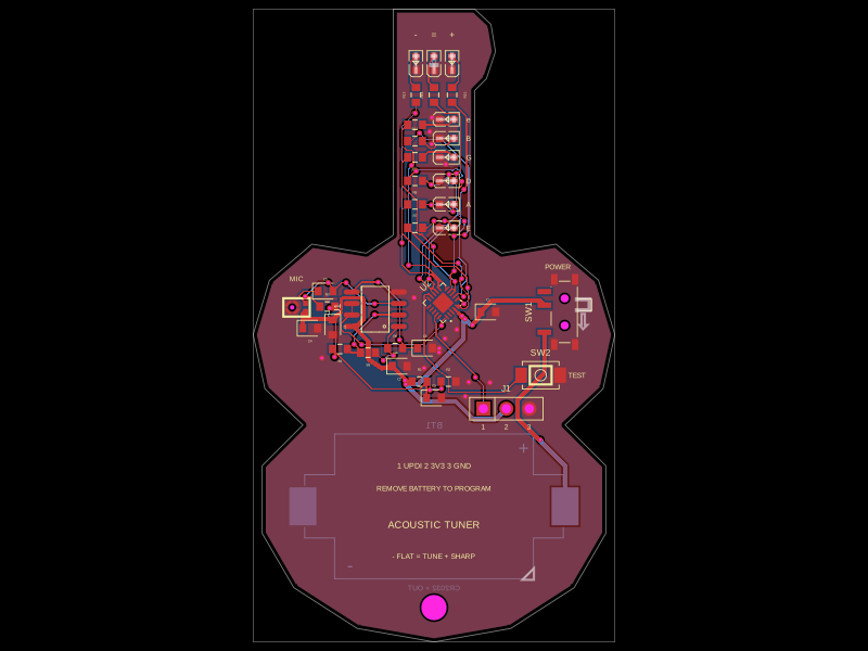 More from this authorgokul/acoustic-guitar-tunerThis code defines the physical pin configuration and footprint layouts for the ATtiny1616 microcontroller and a matching tactile switch component, including their key hardware connection points, dimensions, and 3D models.
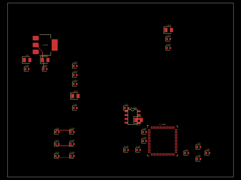 Similar packagecodezonly/pt1This design implements a compact embedded hardware module combining a Seeed XIAO ESP32-C6 microcontroller, a RushFPV GNSS Mini M10 GPS module, and an SX1262 LoRa transceiver, integrated with USB-C power/data, user interface LEDs and buttons, decoupling capacitors, and antenna connectors for GPS and LoRa communication.
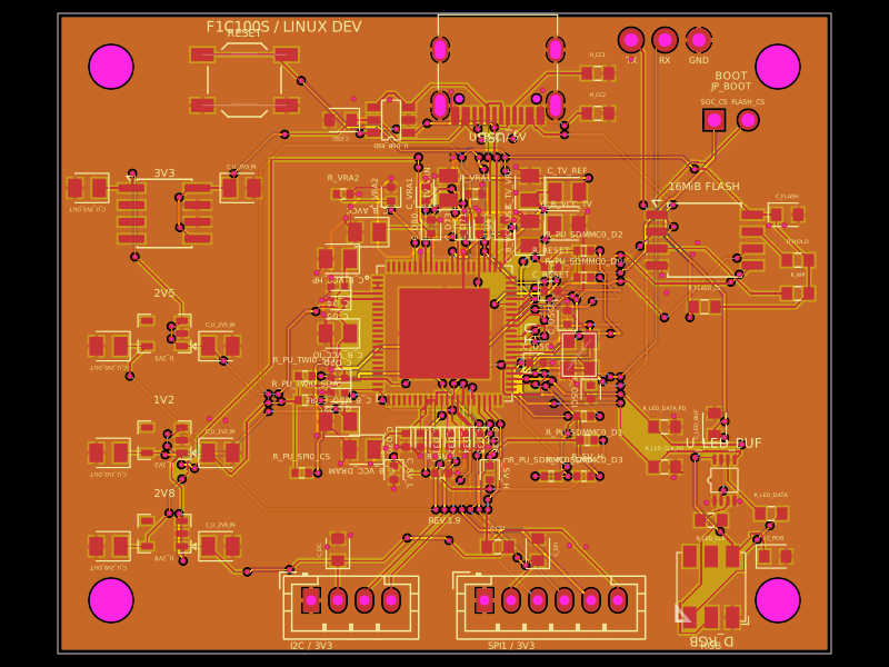 Discover something newseveibar/f1c100s-linux-dev-boardA 4-layer F1C100S Linux development carrier board with USB‑C power/data, multi-rail LDOs, SPI NOR flash, reset/boot interfaces, I²C/SPI/UART headers, ESD protection, and a buffered 5‑V clocked RGB LED.