gokul/lora-device
A compact LoRa/GNSS device PCB integrating an SX1262 radio, GNSS module, USB/UART interface, 1.5 µH inductor, LiPo battery connector with NTC, and supporting passives.
- Version
- 0.1.6
- License
- unset
- Stars
- 0
components/UsbRouting.tsx
// Coordinates in each path are local to its first connected component.
// JLC04161H-7628: 0.24 mm width / 0.16 mm pair gap / 0.20 mm ground gap.
// See docs/jlcpcb-fabrication.md for the stack-up and calculator evidence.
export function UsbRouting() {
  return (
    <>
      <trace
        name="UsbPositiveMain"
        from=".U6 > .pin6"
        to=".R12 > .pin2"
        thickness={0.24}
        pcbPath={[
          {
            x: -0.94996,
            y: 2.4,
          },
          {
            x: -0.94996,
            y: 2.4,
            via: true,
            fromLayer: "top",
            toLayer: "bottom",
          },
          {
            x: -0.94996,
            y: 2.4,
          },
          {
            x: -0.94996,
            y: 3.19996,
          },
          {
            x: -2.55,
            y: 4.8,
          },
          {
            x: -14.7,
            y: 4.8,
          },
          {
            x: -16,
            y: 6.1,
          },
          {
            x: -16,
            y: 14.55,
          },
          {
            x: -16,
            y: 14.55,
            via: true,
            fromLayer: "bottom",
            toLayer: "top",
          },
          {
            x: -16,
            y: 14.55,
          },
        ]}
      />
      <trace
        name="UsbNegativeMain"
        from=".U6 > .pin4"
        to=".R11 > .pin2"
        thickness={0.24}
        pcbPath={[
          {
            x: 0.94996,
            y: 2.4,
          },
          {
            x: 0.94996,
            y: 2.4,
            via: true,
            fromLayer: "top",
            toLayer: "bottom",
          },
          {
            x: 0.94996,
            y: 2.4,
          },
          {
            x: 0.415685,
            y: 2.4,
          },
          {
            x: -2.384315,
            y: 5.2,
          },
          {
            x: -14.534315,
            y: 5.2,
          },
          {
            x: -15.6,
            y: 6.265685,
          },
          {
            x: -15.6,
            y: 12.45,
          },
          {
            x: -15,
            y: 13.05,
          },
          {
            x: -15,
            y: 13.05,
            via: true,
            fromLayer: "bottom",
            toLayer: "top",
          },
          {
            x: -15,
            y: 13.05,
          },
        ]}
      />
      <trace
        name="UsbNegativeMcu"
        from=".R11 > .pin1"
        to=".U1 > .IO19"
        thickness={0.2}
        pcbPath={[".R11 > .pin1", ".U1 > .IO19"]}
      />
      <trace
        name="UsbPositiveMcu"
        from=".R12 > .pin1"
        to=".U1 > .IO20"
        thickness={0.2}
        pcbPath={[".R12 > .pin1", ".U1 > .IO20"]}
      />
      <copperpour
        name="UsbGroundReference"
        layer="inner2"
        connectsTo="net.GND"
        unbroken
        clearance={0.2}
        outline={[
          { x: 1, y: -13 },
          { x: 3.4, y: -13 },
          { x: 3.4, y: -21.8 },
          { x: 4.1, y: -22.5 },
          { x: 16.8, y: -22.5 },
          { x: 20.8, y: -26.5 },
          { x: 20.8, y: -28.3 },
          { x: 16.2, y: -28.3 },
          { x: 16.2, y: -25.8 },
          { x: 14.7, y: -24.3 },
          { x: 2.8, y: -24.3 },
          { x: 1, y: -22.5 },
        ]}
      />
      <via
        name="UsbGroundMcu"
        connectsTo="net.GND"
        pcbX={3.5}
        pcbY={-14}
        holeDiameter={0.3}
        outerDiameter={0.6}
        layers={["top", "bottom"]}
      />
      <via
        name="UsbGroundMid"
        connectsTo="net.GND"
        pcbX={3.5}
        pcbY={-17.5}
        holeDiameter={0.3}
        outerDiameter={0.6}
        layers={["top", "bottom"]}
      />
      <via
        name="UsbGroundTurn"
        connectsTo="net.GND"
        pcbX={14}
        pcbY={-24.8}
        holeDiameter={0.3}
        outerDiameter={0.6}
        layers={["top", "bottom"]}
      />
      <via
        name="UsbGroundEsd"
        connectsTo="net.GND"
        pcbX={20.2}
        pcbY={-25.5}
        holeDiameter={0.3}
        outerDiameter={0.6}
        layers={["top", "bottom"]}
      />
    </>
  );
}
Related Packages
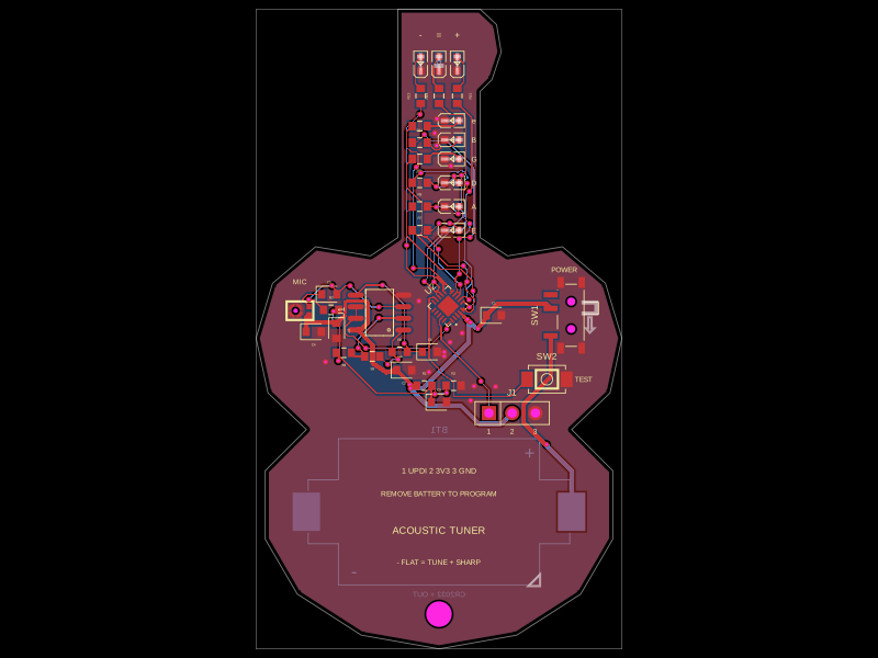 More from this authorgokul/acoustic-guitar-tunerThis code defines the physical pin configuration and footprint layouts for the ATtiny1616 microcontroller and a matching tactile switch component, including their key hardware connection points, dimensions, and 3D models.
 Similar packagecodezonly/pt1This design implements a compact embedded hardware module combining a Seeed XIAO ESP32-C6 microcontroller, a RushFPV GNSS Mini M10 GPS module, and an SX1262 LoRa transceiver, integrated with USB-C power/data, user interface LEDs and buttons, decoupling capacitors, and antenna connectors for GPS and LoRa communication.
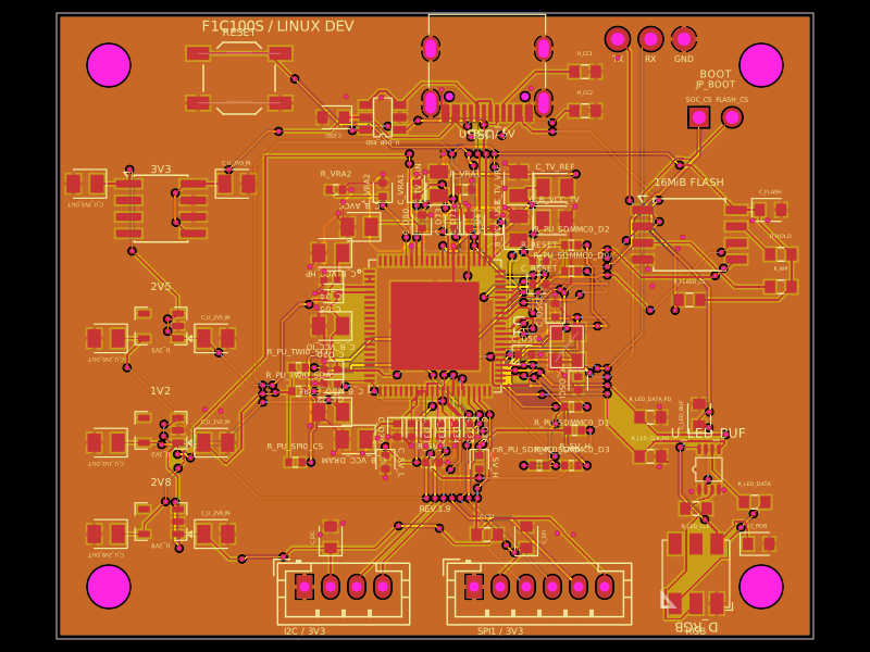 Discover something newseveibar/f1c100s-linux-dev-boardA 4-layer F1C100S Linux development carrier board with USB‑C power/data, multi-rail LDOs, SPI NOR flash, reset/boot interfaces, I²C/SPI/UART headers, ESD protection, and a buffered 5‑V clocked RGB LED.