gokul/flex-led-wristband
A flexible, rechargeable touch wristband PCB with MCP73831 Li-ion charging, switched 3.0 V regulation, ATtiny402 control, TTP223 capacitive touch sensing, and six charlieplexed red LEDs plus power/charge indicators.
- Version
- 0.0.3
- License
- unset
- Stars
- 0
scripts/release.py
"""Audit exported flex geometry and prepare manufacturing references.
Run after tsci build/export and KiCad DRC. Requires gerbonara 1.5.0 and shapely 2.x.
Coordinates are millimetres, board centre origin, +Y up, viewed from top.
"""
import csv
import hashlib
import html
import io
import json
import zipfile
from collections import Counter
from pathlib import Path
from gerbonara.rs274x import GerberFile
from gerbonara.excellon import ExcellonFile
from gerbonara.layers import LayerStack
from shapely.geometry import Point, Polygon, LineString, box
from shapely.ops import unary_union

ROOT = Path(__file__).resolve().parents[1]
DIST = ROOT / 'dist'
circuit = json.loads((DIST / 'index/circuit.json').read_text())
def elements(kind):
    return [element for element in circuit if element['type'] == kind]
def primitive_shape(primitive):
    kind = type(primitive).__name__
    if kind == 'Line':
        return LineString([(primitive.x1,primitive.y1),(primitive.x2,primitive.y2)]).buffer(primitive.width/2,quad_segs=64)
    if kind == 'Rectangle':
        assert primitive.rotation == 0
        return box(primitive.x-primitive.w/2, primitive.y-primitive.h/2, primitive.x+primitive.w/2, primitive.y+primitive.h/2)
    if kind == 'Circle':
        return Point(primitive.x, primitive.y).buffer(primitive.r, quad_segs=64)
    if kind == 'ArcPoly':
        assert not any(primitive.arc_centers), 'Unexpected curved region; review parser'
        return Polygon(primitive.outline)
    raise ValueError(f'Unsupported aperture primitive: {kind}')
def shapes(layer):
    return [primitive_shape(primitive) for obj in layer.objects for primitive in obj.to_primitives()]
def digest(path):
    return hashlib.sha256(path.read_bytes()).hexdigest()

errors = [element for element in circuit if 'error' in element['type']]
assert not errors, errors
board = elements('pcb_board')[0]
outline = Polygon([(point['x'], point['y']) for point in board['outline']])
assert outline.is_valid and outline.area > 0
supports = [box(s['center']['x']-s['width']/2, s['center']['y']-s['height']/2, s['center']['x']+s['width']/2, s['center']['y']+s['height']/2) for s in elements('pcb_stiffener')]
assert all(outline.buffer(.001).covers(s) for s in supports)
for via in elements('pcb_via'):
    copper = Point(via['x'],via['y']).buffer(via['outer_diameter']/2)
    assert any(s.covers(copper) for s in supports), f'Unsupported via: {via}'

archive = zipfile.ZipFile(DIST / 'flex-led-wristband-gerbers.zip')
for csv_name in ['bom.csv','pick_and_place.csv']:
    (DIST/csv_name).write_bytes(archive.read(csv_name))
layers = {}
for filename in archive.namelist():
    if filename.endswith('.gbr'):
        layers[filename] = GerberFile.from_string(archive.read(filename).decode())
    elif filename.endswith('.drl'):
        ExcellonFile.from_string(archive.read(filename).decode())
bottom_copper = unary_union(shapes(layers['B_Cu.gbr']))
for exclusion in elements('pcb_keepout'):
    if exclusion['layers'] != ['bottom']: continue
    centre = exclusion['center']
    area = box(centre['x']-exclusion['width']/2,centre['y']-exclusion['height']/2,centre['x']+exclusion['width']/2,centre['y']+exclusion['height']/2)
    assert bottom_copper.intersection(area).area < 1e-7, f'Bottom copper in keepout: {exclusion}'
mask_shapes = shapes(layers['F_Mask.gbr'])
minimum_web = min(first.distance(second) for i,first in enumerate(mask_shapes) for second in mask_shapes[i+1:])
assert minimum_web >= .5-1e-5, minimum_web
mask = unary_union(mask_shapes)
via_opening_distances = [Point(v['x'],v['y']).distance(mask)-v['hole_diameter']/2 for v in elements('pcb_via')]
assert min(via_opening_distances) >= .2-1e-5, min(via_opening_distances)
assert mask.distance(Point(10,1)) > 2.5, 'Touch electrode is exposed'
assert len(layers['B_Mask.gbr'].objects) == 2, 'Unexpected bottom coverlay windows'
for pad in elements('pcb_smtpad'):
    if pad.get('soldermask_margin',0) < 0:
        assert abs(pad['soldermask_margin']+.35) < 1e-6

report = json.loads((DIST/'kicad-drc.json').read_text())
physical_violations = [violation for violation in report['violations'] if violation['type'] != 'lib_footprint_issues']
assert not physical_violations, physical_violations
assert not report['unconnected_items'], report['unconnected_items']
source = {s['source_component_id']:s for s in elements('source_component')}
pads_by_component = {}
for pad in elements('pcb_smtpad'):
    pads_by_component.setdefault(pad['pcb_component_id'],[]).append(pad)
placements=[]
orientations=[]
groups={}
for component in elements('pcb_component'):
    if component.get('do_not_place'): continue
    part=source[component['source_component_id']]
    name=part['name']; mpn=part['manufacturer_part_number']
    # SW1 body origin is distinct from its asymmetric pad bounding-box centre.
    x,y=(0,11) if name=='SW1' else (component['center']['x'],component['center']['y'])
    pads=pads_by_component[component['pcb_component_id']]
    marker='2' if part['ftype']=='simple_led' else '1'
    marker_pad=next(pad for pad in pads if marker in pad.get('port_hints',[]))
    placements.append([name,f'{x:.4f}',f'{y:.4f}','Top',component['rotation']])
    orientations.append([name,mpn,'Cathode' if marker=='2' else 'Pin 1',f"{marker_pad['x']:.4f}",f"{marker_pad['y']:.4f}",f'{x:.4f}',f'{y:.4f}',component['rotation']])
    groups.setdefault(mpn,[]).append(name)
def write_csv(filename,header,rows):
    with (DIST/filename).open('w',newline='') as file:
        writer=csv.writer(file);writer.writerow(header);writer.writerows(rows)
write_csv('assembly-placement.csv',['Designator','Mid X','Mid Y','Layer','Rotation'],placements)
write_csv('assembly-orientation.csv',['Designator','MPN','Orientation marker','Marker X mm','Marker Y mm','Body centre X mm','Body centre Y mm','Design rotation deg'],orientations)
packages={'ATTINY402-SSN':'SOIC-8','MCP73831T-2ACI/OT':'SOT-23-5','MCP1700T-3002E/TT':'SOT-23-3','TTP223-BA6':'SOT-23-6','JS102011SAQN':'9 x 3.6 mm right-angle SMT'}
write_csv('assembly-bom.csv',['Designator','Quantity','Manufacturer Part Number','Package'],[[','.join(refs),len(refs),mpn,packages.get(mpn,'0603 / 1608 metric')] for mpn,refs in groups.items()])
# Fabrication ZIP only: do not let an uncalibrated assembly CSV imply automatic PCBA approval.
with zipfile.ZipFile(DIST/'jlcpcb-fabrication.zip','w',zipfile.ZIP_DEFLATED) as output:
    names={'B_Stiffener_fr4.gbr':'fr4b_0.4.gbr','B_Stiffener_polyimide.gbr':'pib_0.2.gbr'}
    for filename in archive.namelist():
        if filename.endswith(('.gbr','.drl')): output.writestr(names.get(filename,filename),archive.read(filename))
    output.write(ROOT/'FABRICATION.txt','FABRICATION.txt')

# Engineering drawing: all geometry in top-view coordinates, bottom stiffeners dashed.
svg=['<svg xmlns="http://www.w3.org/2000/svg" width="1440" height="820" viewBox="0 0 1440 820">','<rect width="1440" height="820" fill="white"/>','<style>text{font-family:Arial,sans-serif;fill:#15283b}</style>']
def label(x,y,text,size=16,color='#15283b'):
    svg.append(f'<text x="{x}" y="{y}" font-size="{size}" style="fill:{color}">{html.escape(text)}</text>')
label(50,40,'FLEX LED WRISTBAND — ASSEMBLY / FLEX SUPPORT',26)
label(50,69,'Top view • millimetres • board-centre origin • +X right, +Y up • all components on top',17)
scale=14
cx,cy=720,330
def xy(x,y):return cx+scale*x,cy-scale*y
points=' '.join(f'{xy(p["x"],p["y"])[0]},{xy(p["x"],p["y"])[1]}' for p in board['outline'])
svg.append(f'<polygon points="{points}" fill="#fff6c9" stroke="#78651b" stroke-width="2"/>')
for stiffener in elements('pcb_stiffener'):
    x,y=xy(stiffener['center']['x']-stiffener['width']/2,stiffener['center']['y']+stiffener['height']/2)
    svg.append(f'<rect x="{x}" y="{y}" width="{stiffener["width"]*scale}" height="{stiffener["height"]*scale}" fill="#addde7" fill-opacity=".3" stroke="#1684a3" stroke-dasharray="7 5"/>')
for component in elements('pcb_component'):
    part=source[component['source_component_id']];name=part['name']
    for pad in pads_by_component[component['pcb_component_id']]:
        x,y=xy(pad['x'],pad['y'])
        if pad['shape']=='circle': svg.append(f'<circle cx="{x}" cy="{y}" r="{pad["radius"]*scale}" fill="#cfaf53"/>')
        else: svg.append(f'<rect x="{x-pad["width"]*scale/2}" y="{y-pad["height"]*scale/2}" width="{pad["width"]*scale}" height="{pad["height"]*scale}" fill="#cfaf53" stroke="#85651b" stroke-width=".5"/>')
    x,y=xy(component['center']['x'],component['center']['y'])
    text_name={'J_BAT_P':'BAT+','J_BAT_N':'BAT−','J_5V':'5V','J_0V':'GND','J_UPDI':'UPDI','J_VREF':'3V','J_GND':'GND','J_TOUCH':'TOUCH'}.get(name,name)
    label(x-len(text_name)*3.5,y-19 if name!='SW1' else y-30,text_name,13)
for row in orientations:
    if not row[0].startswith(('U','D','SW')):continue
    x,y=xy(float(row[3]),float(row[4]))
    svg.append(f'<circle cx="{x}" cy="{y}" r="4" fill="#c32b47"/>')
    label(x+6 if row[2]=='Cathode' else x-12,y-6 if row[2]=='Cathode' else y+5,'K' if row[2]=='Cathode' else '1',12,'#c32b47')
x,y=xy(-4.5,12.8)
svg.append(f'<rect x="{x}" y="{y}" width="126" height="50.4" fill="none" stroke="#15283b" stroke-width="2"/>')
label(50,605,'90 × 32 mm outline; 10 mm wings. Dashed blue = bonded bottom stiffener, not a copper layer.',18)
label(50,638,'Centre: 30 × 30 mm FR4, 0.40 mm + 0.05 mm adhesive. LED islands: 6 × 8 mm PI, 0.20 mm + adhesive.',18)
label(50,671,'Red dot = IC/switch pin 1 or LED cathode K. See assembly-orientation.csv for exact marker coordinates.',18)
label(50,704,'Bend gently only between supports; minimum intended radius 12 mm, subject to factory approval. No creases.',18)
label(50,737,'SW1 body centre (0, 11); pin 1 (2.5, 8.25). ON = 2–3, OFF = 1–2. Check before connecting a cell.',18)
label(50,780,'Assembly review required: match package marks and supplier rotations. Battery and strap are external.',17)
svg.append('</svg>');(DIST/'assembly.svg').write_text('\n'.join(svg))
stack=LayerStack.open(DIST/'flex-led-wristband-gerbers.zip')
for side in ['top','bottom']:
    (DIST/f'gerber-{side}.svg').write_text(str(stack.to_pretty_svg(side=side)))
summary={'circuit_errors':0,'circuit_warnings':dict(Counter(e['type'] for e in circuit if 'warning' in e['type'])),'kicad_unconnected':0,'kicad_physical_violations':0,'kicad_library_notices':len(report['violations']),'coverlay_minimum_web_mm':round(minimum_web,4),'via_hole_to_coverlay_opening_minimum_mm':round(min(via_opening_distances),4),'vias':len(elements('pcb_via')),'all_via_pads_supported':True,'placed_components':len(placements),'outline_valid':True,'circuit_sha256':digest(DIST/'index/circuit.json'),'gerber_zip_sha256':digest(DIST/'flex-led-wristband-gerbers.zip'),'jlcpcb_zip_sha256':digest(DIST/'jlcpcb-fabrication.zip')}
(DIST/'manufacturing-checks.json').write_text(json.dumps(summary,indent=2)+'\n')
print(json.dumps(summary,indent=2))
Related Packages
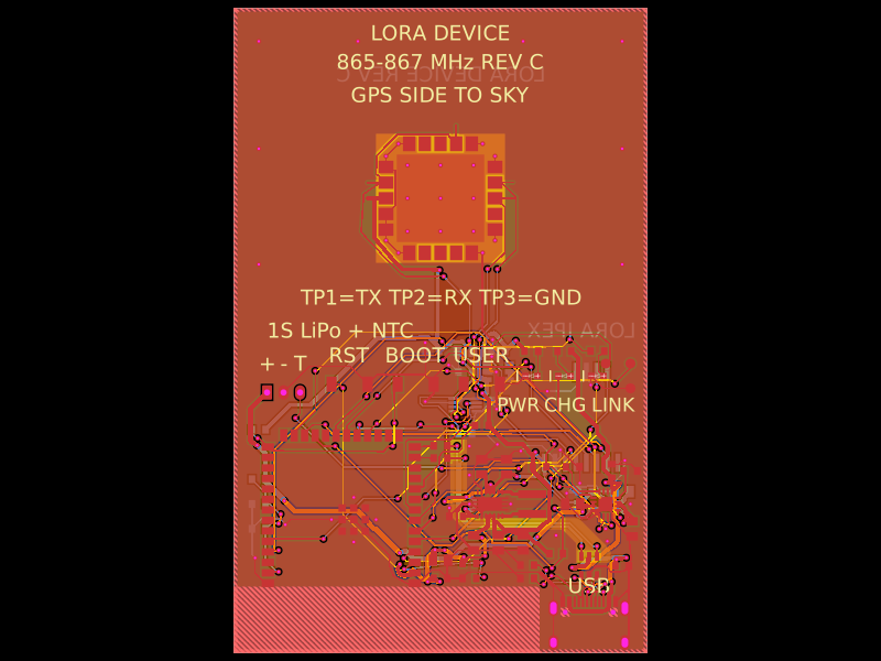 More from this authorgokul/lora-deviceA compact LoRa/GNSS device PCB integrating an SX1262 radio, GNSS module, USB/UART interface, 1.5 µH inductor, LiPo battery connector with NTC, and supporting passives.
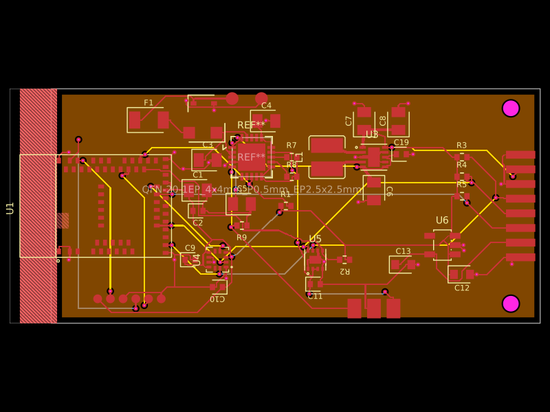 Similar packagemohan-bee/fitness-bandA 4-layer BLE wearable mainboard with Li-ion charging/protection, 3.3/1.8 V power regulation, motion and battery sensing, plus a folded 2-layer flex sensor board carrying MAX30102 optical and TMP117 temperature sensors.
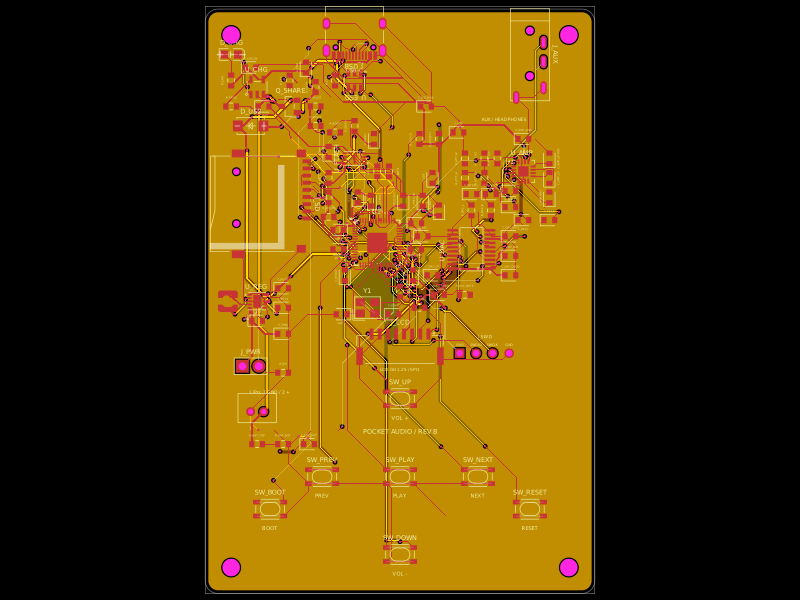 Discover something newDevesh36/pocket-audio-playerA portable, rechargeable microSD audio player built around an RP2040, SPI flash, USB‑C charging/power management, LCD/button controls, PCM5102A I²S DAC, and TPA6132A headphone amplifier in a 3D‑printed enclosure.